You are currently viewing SemiWiki as a guest which gives you limited access to the site. To view blog comments and experience other SemiWiki features you must be a registered member. Registration is fast, simple, and absolutely free so please,
join our community today!
The TSMC Open Innovation Platform® (OIP) Ecosystem Forum brings TSMC’s design ecosystem member companies together to share with our customers real-case solutions for customers’ design challenges and success stories of best practice in TSMC’s design ecosystem.
More than 90% of the attendees last year said “this… Read More
You will never meet a more approachable CEO in the semiconductor ecosystem than Dr. Walden C. Rhines. The first time I met Wally was way back when I blogged for food and he invited me over for lunch. Even better, a year or two later I was having dinner with a friend at the DBL Tree in San Jose. Wally was waiting for his flight home so he joined… Read More
At TSMC’s Open Innovation Platform (OIP) Ecosystem Forum, Mentor made technical presentations on four different topics, two of them co-presented with TSMC and LSI Corporation. Those presentations are described below with links to downloadable pdf presentation files.
Finding and Fixing Double Patterning Errors in… Read More
Silicon Creations will be presenting a paper with Berkeley Design Automation at the TSMC Open Innovation Platform (OIP) Ecosystem Forum next week where TSMC’s design ecosystem member companies and customers share real-case solutions for design challenges within TSMC’s design ecosystem:
This presentation will describe … Read More
The TSMC Open Innovation Platform® (OIP) Ecosystem Forum brings TSMC’s design ecosystem member companies together to share with our customers real-case solutions for customers’ design challenges and success stories of best practice in TSMC’s design ecosystem.
More than 90% of the attendees last year said “this… Read More
The TSMC Open Innovation Platform® (OIP) Ecosystem Forum brings TSMC’s design ecosystem member companies together to share with our customers real-case solutions for customers’ design challenges and success stories of best practice in TSMC’s design ecosystem. More than 90% of the attendees last year said “this… Read More
GlobalFoundries did a nice response to my “How has 20nm Changed the Semiconductor Ecosystem?” and redefined the word collaboration. Our industry is plagued with sound bites and acronyms so let us agree on a semiconductor ecosystem definition of collaboration.
Mojy Chianis senior vice president, design enablement at… Read More
During my annual holiday meal with one of my favorite EDA icons some rather bold predictions were made. On his side it was more of what he would LIKE to see happen, on my side it was more of what will HAVE to happen for the semiconductor ecosystem to thrive in the coming years.
Mike Gianfagna (Viva Italia!) spent 15+ years with RCA/GE Semiconductor… Read More
LVS Challenges at Advanced Nodes
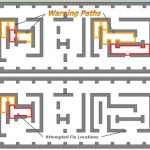
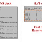
Accurate, comprehensive device recognition, connectivity extraction, netlist generation and, ultimately, circuit comparison becomes more complex with each new process generation. As the number of layers and layer derivations increases the complexity of devices, especially Layout Dependent… Read More
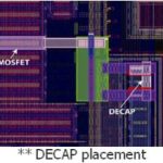
Preventing electrical circuit failure is a growing concern for IC designers today. Certain types of failures such as electrostatic discharge (ESD) events, have well established best practices and design rules that circuit designers should be following. Other issues have emerged more recently, such as how to check circuits… Read More