TCAD Update from Synopsys

TCAD Update from Synopsys
by Daniel Payne on 11-03-2025 at 10:00 am

TCAD importance min

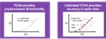
We live in an exploding AI world, and this has put pressure on foundries to deliver new products faster than ever before. Any help to accelerate the semiconductor R&D goes a long way to make the life of Fab engineers easier. EDA tools in the TCAD (Technology Computer Aided Design) category are critical for TCAD engineers to accelerating… Read More


ASU Silvaco Device TCAD Workshop: From Fundamentals to Applications

ASU Silvaco Device TCAD Workshop: From Fundamentals to Applications
by Daniel Nenni on 10-21-2025 at 10:00 am

SILVACO ASU Workshop 400x400

The ASU-Silvaco Device Technology Computer-Aided Design Workshop is a pivotal educational and professional development event designed to bridge the gap between theoretical semiconductor physics and practical device engineering. Hosted by Arizona State University in collaboration with Silvaco, a leading provider of … Read More


Webinar: ASU-Silvaco Device TCAD Workshop: From Fundamentals to Applications

Webinar: ASU-Silvaco Device TCAD Workshop: From Fundamentals to Applications
by Admin on 10-15-2025 at 6:05 pm

This workshop is a fast-paced, one-day program led by Prof. Dragica Vasileska and Prof. Stephen M. Goodnick. Spend the morning grounding yourself in semiconductor physics and transport, then transition in the afternoon to instructor-led, hands-on Silvaco TCAD labs (e.g., MOS Capacitors, MOSFETs, SOI Devices, FinFETs).… Read More


Simulating Gate-All-Around (GAA) Devices at the Atomic Level

Simulating Gate-All-Around (GAA) Devices at the Atomic Level
by Daniel Payne on 09-17-2025 at 10:00 am

GAA FET min

Transistor fabrication has spanned the gamut from planar devices o FinFET to Gate-All-Around (GAA) as silicon dimensions have decreased in the quest for higher density, faster speeds and lower power. Process development engineers use powerful simulation tools to predict and even optimize transistor performance for GAA devices.… Read More


Silvaco’s Diffusion of Innovation: Ecosystem Investments Driving Semiconductor Advancements

Silvaco’s Diffusion of Innovation: Ecosystem Investments Driving Semiconductor Advancements
by Admin on 06-27-2025 at 8:00 am

Silvaco at a Glance 2025

In Silvaco’s June 2025 Tech Talk, “The Diffusion of Innovation: Investing in the Ecosystem Expansion,” Chief Revenue Officer Ian Chen outlined how strategic partnerships accelerate R&D in semiconductor design and digital twin modeling. As a leading provider of TCAD, EDA software, and SIP solutions,… Read More


Silvaco at the 2025 Design Automation Conference #62DAC

Silvaco at the 2025 Design Automation Conference #62DAC
by Daniel Nenni on 06-16-2025 at 8:00 am

62nd DAC SemiWiki

Please join us at the Design Automation Conference 2025 where we will highlight the company’s wide range of EDA products and semiconductor IP  targeting, Power Devices, Automotive, Memory, Displays, HPC, 5G / 6G, and IoT applications.

When: June 23 – 25, 2025, Exhibit Hours: 10:00 AM PDT – 6:00 PM PDT

Where: Moscone Center West,… Read More


TCAD for 3D Silicon Simulation

TCAD for 3D Silicon Simulation
by Daniel Payne on 06-03-2025 at 10:00 am

Silvaco TCAD min

Semiconductor fabs aim to have high yields and provide processes that attract design firms and win new design starts, but how does a fab deliver their process nodes in a timely manner without having to run lots of expensive silicon through the line? This is where simulation and TCAD tools come into play, and to learn more about this… Read More


Intel Foundry Delivers!

Intel Foundry Delivers!
by Daniel Nenni on 05-05-2025 at 10:00 am

Intel Foundry Direct Connect Hall 4 1024x576

Now that the dust has settled, I will give you my take on the Intel Foundry event. Some might call me a semiconductor event critic as I have attended hundreds of them over the last 40 years starting with the Design Automation Conference in 1984. Foundry events are my favorite because they really are the pulse of the semiconductor industry,… Read More


Understanding Sheath Behavior Key to Plasma Etch

Understanding Sheath Behavior Key to Plasma Etch
by Scott Kruger on 08-11-2022 at 10:00 am

Final Edit EtchingProcess Illustration

Readers of SemiWiki will be well aware of the challenges the industry has faced in photolithography in moving to new nodes, which drove the development of new EUV light sources as well as new masking techniques.  Plasma etching is another key step in chip manufacturing that has also seen new challenges in the development of new sub-10nm… Read More


SISPAD – Cost Simulations to Enable PPAC Aware Technology Development

SISPAD – Cost Simulations to Enable PPAC Aware Technology Development
by Scotten Jones on 10-31-2021 at 10:00 am

Slide11

I was invited to give a plenary address at the SISPAD conference in September 2021. For anyone not familiar with SISPAD it is a premiere TCAD conference. This year for the first time SISPAD wanted to address cost and my talk was “Cost Simulations to Enable PPAC Aware Technology Development”.

For many years the standard in technology… Read More