I have previously written about SPIE day 1 and 2 so I want to wrap up my coverage with some impressions from days 3 and 4. My single biggest take away from the conference is that EUV has made tremendous progress in the last 12 months. Last year the mood of the conference was in my opinion pessimistic with respect to EUV, this year the mood… Read More

Tag: spie
Mapping Focus and Dose onto BEOL Fabrication Effects
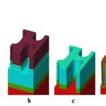
With today’s ArF based lithography using 193nm wavelength light, we are hard up against the limitations imposed by the Raleigh equation. Numerous clever things have been devised to maximize yield and reduce feature size. These include 2 beam lithography, multiple patterning, immersion litho processes to improve NA, thinner… Read More
SPIE Advanced Lithography Preview
Next week is the SPIE Advanced Lithography Conference in San Jose, the premier conference for advanced lithography used to produce state-of-the-art semiconductors. Last year I blogged after the conference about some of the key points I heard at the conference and this year I plan to do the same.
What’s Hot at SPIE Advanced Lithography

The 40[SUP]th[/SUP] SPIE Advanced Lithography conference will be at the San Jose Convention Center 22-26 February. Over the past few years, this conference has grown in scope to include emerging patterning technologies, like directed self-assembly (DSA) and design-process-technology co-optimization.
Underlying all … Read More
SEMICON Update: 450mm, EUV, FinFET, and More
I spent all of last week at SEMICON West meeting with customers, potential customers, partners and various industry analysts and experts. I was involved in many interesting discussions over the course of the week and I thought I would share some of the more interesting observations:
Alternate Fin Materials Pushed Out
I have for… Read More
450mm Delayed and Other SPIE News
Last week I attended the SPIE Advanced Technology Conference. There were a lot of interesting papers and as is always the case at these conferences, there was a lot of interesting things to learn from talking to other attendees on the conference floor.
The first interesting information from the conference floor was that 450mm is… Read More
It’s a 14nm photomask, what could possibly go wrong?
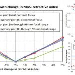
Let’s start with the bottom line: in 14nm processes, errors which have typically been little more than noise with respect to photomask critical dimension (CD) control targets at larger process nodes are about to become very significant, even out of control if not accounted for.… Read More
Magic? No! It’s Computational Lithography

The industry plans to use 193nm light at the 20nm, 14nm, and 10nm nodes. Amazing, no? There is no magic wand; scientists have been hard at work developing computational lithography techniques that can pull one more rabbit out of the optical lithography hat.
Tortured metaphors aside, the goal for the post-tapeout flow is the same… Read More
Get the Latest Info on DFM at the SPIE Litho Conference
While the SPIE Advanced Lithography conference is best known for IC manufacturing, computational lithography, mask preparation and other back-end topics, there is also a significant amount of interest in Design for Manufacturing (DFM) at the conference because some litho issues are best (or only) addressed by modifying the… Read More
DFM Industry Survey
As part of the DFM Conference at the SPIE Advance Lithography symposium, the DFM committee is conducting an informal survey on the current state of Design For Manufacturability in the Semiconductor Industry.
Please take this anonymous 16 question survey to identify critical Design for Manufacturability (DFM) issues facing… Read More