You are currently viewing SemiWiki as a guest which gives you limited access to the site. To view blog comments and experience other SemiWiki features you must be a registered member. Registration is fast, simple, and absolutely free so please,
join our community today!
By Zameer Mohammed
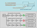
This article claims to provide clear key insights of Min Pulse Width (MPW) timing signoff check, proactive closure strategies for faster time-to-market, and effective methods to prevent silicon failures.
Min Pulse Width (MPW) check for timing signoff has become an important design constraint at the sub-5nm… Read More
Artificial intelligence (AI) and machine learning (ML) are hot topics. Beyond the impact these technologies are having on the world around us, they are also having impact on the semiconductor and EDA ecosystem. I posted a blog last week that discussed how Cadence views AI/ML, both from a tool and ecosystem perspective. The is one… Read More
I had the opportunity to preview an upcoming webinar on SemiWiki that deals with design robustness for signoff regarding advanced node digital designs (think single-digit nanometers). “Design robustness” is a key term – it refers to high quality, high yielding SoCs that come up quickly and reliably in the target system. We all… Read More
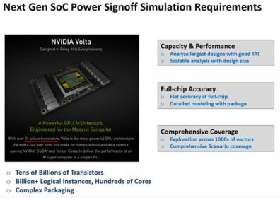
Want to know how NVIDIA signs off on power integrity and reliability on mega-chips? Read on.
PPA over-design has repercussions in increased product cost and potential missed schedules with no guarantee of product success. Advanced SoCs pack more functionality and performance resulting in higher power density, but traditional… Read More
At the most basic level, semiconductor design is all about transistors. Any report on a large microprocessor or mobile application processor is in awe about how many transistors it contains. Moore’s Law is all about the most economic way to manufacture transistors. Each process generation for the last decade and looking ahead… Read More
In an SoC world driven by IP, where an SoC can have hundreds of IP (sourced not only from 3[SUP]rd[/SUP] party but also from internal business units which can have a lot of legacy) integrated together, it has become essential to have a comprehensive and standard method to verify and signoff the IP. Additionally, these checks must … Read More
With the unprecedented increase in semiconductor design size and complexity design teams are required to accommodate multiple design constraints such as multiple power domains for low power design, multiple modes of operation, many clocks running, and third party IPs with different SDCs. As a result timing closure has become… Read More
In the semiconductor design industry, most of the designs are created and optimized at the RTL level, mainly through home grown scripts or manual methods. As there can be several iterations in optimizing the hierarchy for physical implementation, it’s too late to do the hierarchical optimizations after reaching the floor plan… Read More
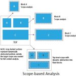
The semiconductor design sizes, these days, can easily be of the order of several hundred millions of cells, adding into the complexity of verification. Amid ever growing design sizes, it’s a must that the timing verification is done accurately. Normally Static Timing Analysis (STA) is done to check whether all clocks and signals… Read More
Yesterday Cadence had an all-day Signoff Summit where they talked about the tools that they have for signoff in advanced nodes. Well, of course, those tools work just fine in non-advanced nodes too, but at 20nm and 16nm there are FinFETs, double patterning, timing impacts from dummy metal fill, a gazillion corners to be analyzed… Read More