You are currently viewing SemiWiki as a guest which gives you limited access to the site. To view blog comments and experience other SemiWiki features you must be a registered member. Registration is fast, simple, and absolutely free so please,
join our community today!
It was not really a surprise to learn that, finally, MIPS have been sold, as the company was officially for sale since April 2012. Nevertheless, the interesting part of this news comes from the buyer’ identity: Imagination Technologies. Imagination is an UK based company, like ARM, selling processor IP cores, like ARM, but the … Read More
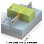
The common theme amongst semiconductor ecosystem conferences this year is FinFETS, probably the most exciting technology we will see this decade. A lot has been written on SemiWiki about FinFETS, it is one of the top trending search terms, but there is some confusion about the process naming so let me attempt to explain.
In planar… Read More
Our EDA industry loves three letter acronyms so credit the same industry for creating a five letter acronym CoWoS. Two weeks ago TSMC announced tape-out of their first CoWoS test chip integrating with JEDEC Wide I/O mobile DRAM interface, making me interested enough to read more about it. At the recent TSMC Open Innovation Platform… Read More
Electromigration (EM) is a reliability concern for IC designers because a failure in the field could spell disaster as in lost human life or even bankruptcy for a consumer electronics company. In the old days of IC design we would follow a sequential and iterative design process of:… Read More
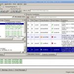
Jasper Apps White Paperby Paul McLellan on 11-01-2012 at 7:30 pmCategories: EDA
Just in time for the Jasper User Group meeting, Jasper have a new white paper explaining the concept of JasperGold Apps.
First the User Group Meeting. It is in Cupertino at the Cypress Hotel November 12-13th. For more details and to register, go here. The meeting is free for qualified attendees (aka users). One thing I noticed at the… Read More
On Halloween, Atrenta and TSMC announced the availability of SpyGlass IP Kit 2.0. IP Kit is a fundamental element of TSMC’s soft IP9000 Quality Assessment program that assesses the robustness and completeness of soft (synthesizable) IP.
IP Kit 2.0 will be fully supported on TSMC-Online and available to all TSMC’s soft IP alliance… Read More
ARM and a LEGby Paul McLellan on 11-01-2012 at 5:09 pmCategories: Arm, IP
I went to Warren East’s keynote speech at ARM Techcon today. There had been some hints earlier in the week that some significant announcements would be made and, while they were not earth-shattering, I think that they will be significant in the long term.
One interesting thing that Warren pointed out is that the ARM partner… Read More
An announcement at the ARM conference was of a joint project to tape out an ARM Cortex-M0 in IBM’s 14nm FinFET process. In fact they taped out 3 different versions of the chip using different routing architectures to see the impact on yield.
This was the first 14nm ARM tapeout, it seems. I’m sure Intel has built plenty … Read More
Jasper restructured JasperGold so that it could deliver its formal technology more flexibly by having a base system and a porfolio of apps. This would also make it easier to upgrade capabilities by creating new apps. Today, Jasper announced two new apps:
- JasperGold Structural Property Synthesis (SPS)
- JasperGold Behavioral
…
Read More
At DAC in June I visited and blogged about 30+ EDA and Semi IP companies, however I didn’t have time to watch the TowerJazz presentation in the Cadence Theater entitled: AMS Flow for Power Management Designs. Today I watched the 26 minute video and have summarized what I learned in this blog post.… Read More