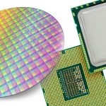
Moore’s is still the law, and device scaling remains the key focus of front-end process research, however next-generation technologies–and the Big Data, cloud computing world that supports mobile, IoT, and other next-gen applications–are the new drivers, bringing new demands and challenges running … Read More

Tag: semiconductor
Virtual Fabrication: Not just for fabs. Fabless companies can benefit from more visibility into process technology
Ever since I started talking about Virtual Fabrication I have mostly looked at it from the manufacturers’ perspective, where it has obvious benefits to develop and model new process technology. But what about the fabless design concept and indeed even the semiconductor IP world that has spawned from it as well? It seems that Virtual… Read More
Intel’s Manufacturing Lead Explained
The calls from Wall Street keep coming with basically the same set of questions: “Does Intel really have a 2-3 year process lead? Can Intel lead the foundry segment? Can Intel Lead the Mobile SoC Segment?” The feeling amongst the buy and sell side investment people is that unless Intel can lead a market they will not stay in it… Read More
Calypto @ #51DAC Must See!
DAC 2014 in San Francisco promises plenty of new information on emerging low power techniques and faster ways to get to working, fully verified RTL using high level synthesis and formal verification. Get the latest from the industry leader in technologies for high level design and verification and low power RTL designby attending… Read More
eSilicon @ #51 DAC – Why is a Chip Company at DAC?
eSilicon is a fabless chip company that is credited with starting the fabless ASIC movement. You can read more about them in the ASIC chapter of SemiWiki’s new book on the fabless semiconductor industry. But why would a fabless ASIC company come to DAC?
At one level, eSilicon starts where EDA technology ends – taking a taped out chip… Read More
Concept Engineering Showcases Effective SoC Debugging Techniques

In a complex environment of semiconductor design where an SoC can have several millions of gates and multiple number of IPs at different levels of abstractions from different sources integrated together, it becomes really difficult to understand and debug the overall SoC design. Of course, along with the SoC integration, optimization… Read More
Atmel and the Arduino Zero
As I wrote about last month, this weekend is the Maker Faire in San Mateo. If you are interested in the cutting edge of what people are getting up to outside of the corporate world, this is the place to go. You will see stuff that you will not hear about for a year or two when it finally goes mainstream.
Increasingly, there is a lot of electronics… Read More
Taming The Challenges of SoC Testability
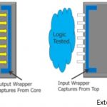
With the advent of large SoCs in semiconductor design space, verification of SoCs has become extremely challenging; no single approach works. And when the size of an SoC can grow to billions of gates, the traditional methods of testability of chips may no longer remain viable considering the needs of large ATPG, memory footprint,… Read More
A Brief History of MunEDA

In 2002, MunEDA was launched under the guidance of EDA academic veterans and IEEE fellows Prof. Kurt Antreich and Prof. Helmut Gräb (TUM Munich Technical University ) which represented 20 plus years of EDA research and experience. All MunEDA tools are combined in a tool suite called WiCkeD[SUP]TM[/SUP]. The tool suite brand was… Read More
New Frontiers in MEMS and Their Enablers

With the 51[SUP]st[/SUP] DACapproaching quickly, I spent some time last week-end to look around about what new trends, technologies and innovations will be most talked about during DAC. Every year, I find some exciting new technologies in the semiconductor industry and the overall semiconductor ecosystem that get wider exposure… Read More