Introduction
Mentor Graphics and GLOBALFOUNDRIES have been working together for several generations since the 65nm node on making IC designs yield higher. Michael Buehler-Garcia, director of Calibre Design SolutionsMarketing at Mentor Graphics spoke with me by phone today to explain how they are working with GLOBALFOUNDRIES… Read More

Tag: semiconductor
20nm SoC Design

There are a large number of challenges at 20nm that didn’t exist at 45nm or even 32nm.
The biggest issues are in the lithography area. Until now it has been possible to make a reticle using advanced reticle enhacement technology (RET) decoration and have it print. Amazing when you think that at 45nm we are making 45nm features… Read More
Silicon One

I have talked quite a bit over the last few years about how the trend towards small consumer devices with very fast ramp times. For example, pretty much any time Apple introduces a new product line (iPod, iPhone, iPad…) it becomes the fastest growing market in history. This has major implications for semiconductor design … Read More
Reducing SoC Power Consumption using Integrated Voltage Regulators
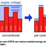
Last month I had the pleasure of meeting Mr Wonyoung Kim, a PhD candidate from Harvard University. Like many candidates, Wonyoung is shopping his thesis for capital in hopes of starting a semiconductor IP company. Here is a brief summary of the technology, please provide appropriate feedback and let’s see if we can get him… Read More
August 11th – Hands-on Workshop with Calibre: DRC, LVS, DFM, xRC, ERC
I’ve blogged about the Calibre family of IC design tools before:
Smart Fill replaced Dummy Fill Approach in a DFM Flow
DRC Wiki
Graphical DRC vs Text-based DRC
Getting Real time Calibre DRC Results with Custom IC Editing
Transistor-level Electrical Rule Checking
Who Needs a 3D Field Solver for IC Design?
Prevention is Better… Read More
Chip-Package-System Webinar
The webinar on CPS (chip-package-system) is on Tuesday 9th August at 11am Pacific time. It will be conducted by Christopher Ortiz, Principal Application Engineer at Apache Design Solutions. Dr. Ortiz has been with Apache since 2007, supporting the Sentinel product line. Prior to Apache he worked at Agere / LSI, where he investigated… Read More
Totem webinar: Analog/Mixed-Signal Power Noise and Reliability

The Totem webinar will be at 11am on Tuesday 2nd August. This session will be conducted by Karan Sahni, Senior Applications Engineer at Apache Design Solutions. Karan has been with Apache since 2008, supporting the Redhawk, Totem, Sentinel product lines. He received his MS in Electrical Engineering from the Syracuse University… Read More
CDNS EDA360 is DEAD!
Hard to believe EDA360, the Cadence Blueprint toBattle ‘Profitability Gap’; Counters Semiconductor Industry’s Greatest Threat!, is DEAD at the ripe old age of one. As you may have already read John Bruggeman left Cadence after the company conference call last week. The formal announcement should go out on Monday after the SEC… Read More
Global Technology Conference 2011

Competition is what made the semiconductor industry and semiconductors themselves what they are today! Competition is what drives innovation and keeps costs down. Not destructive competition, where the success of one depends on the failure of another, but constructive competition that promotes mutual survival and growth… Read More
Intel Briefing: Tri-Gate Technology and Atom SoC

Sorry to disappoint but my 2 hours at the Intel RNB was a very positive experience. It is much more fun writing negative things about industry leaders because I enjoy the resulting hate mail and personal attacks, but the candor and transparency of the Intel guys won me over. They even asked ME questions which was a bit telling. I also… Read More