You are currently viewing SemiWiki as a guest which gives you limited access to the site. To view blog comments and experience other SemiWiki features you must be a registered member. Registration is fast, simple, and absolutely free so please,
join our community today!
Our friends at Threshold Systems have a new class that may be of interest to you. It’s an updated version of the Advanced CMOS Technology class held last May. As part of the previous class we did a five part series on The Evolution of the Extension Implant which you can see on the Threshold Systems SemiWiki landing page HERE. And… Read More
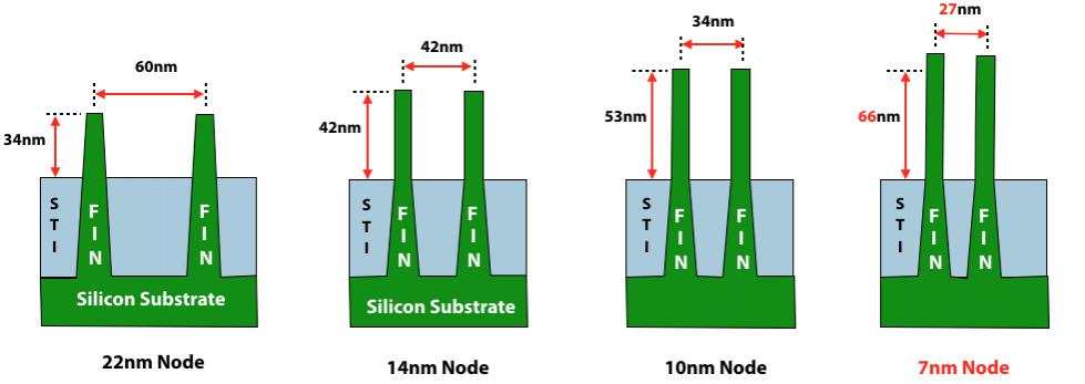
The use of hard masks instead of photoresist for the Extension implant is an effective way to optimize the amount of dopant that is retained along the fin sidewalls for those fins that border along photoresist edges (as discussed in Part 1 of this series).
However, hard masks do nothing to address the dominant problem driving steeper… Read More
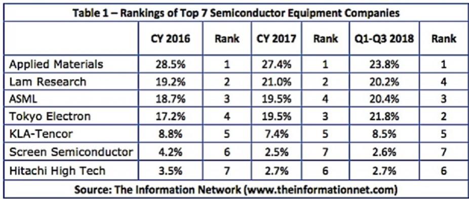
Semiconductor equipment vendor ranking, which didn’t change much between 2016 and 2017, is undergoing a makeover, as Lam Research, ASML, and Tokyo Electron (TEL) are switching places and top-ranked Applied Materials is getting closer to losing its number one ranking.
Since the 1990s, Applied Materials has been the market leader… Read More
On their first quarter earnings call Intel announced that volume production of 10nm has been moved from the second half of 2018 to 2019 due to yield issues. Specifically, they are shipping 10nm in low volume now, but yield improvement has been slower than anticipated. They report that they understand the yield issues but that improvements… Read More
At the SPIE Advanced Lithography Conference imec published a number of papers on EUV, multi-patterning and other lithography issues. In addition to seeing several of the papers presented I had a chance to sit down with imec’s director of advanced patterning, Greg McIntyre. In this article I will summarize my discussions… Read More
As feature sizes have shrunk, the semiconductor industry has moved from simple, single-exposure lithography solutions to increasingly complex resolution-enhancement techniques and multi-patterning. Where the design on a mask once matched the image that would be produced on the wafer, today the mask and resulting image … Read More
At the ISS Conference in January, An Steegen EVP of Semiconductor Technology & Systems at imec gave a talk entitled “Patterning Options for Advanced Technology Nodes”. I was present for her talk and had the opportunity to have a follow up interview with An.… Read More
For me personally EUV has been something of a roller coaster ride over the last several years. I started out a strong believer in EUV but then at the SPIE Advanced Lithography Conference in 2014 TSMC gave a very negative assessment of EUV, and there was a SEMATECH paper on high NA EUV that struck me as extremely unlikely to succeed. I … Read More
For more than a decade 2D NAND has been the leading driver of lithography shrinks, for example, Samsung went from 120nm in 2003 to 16nm in 2014 with shrinks on an almost yearly basis, but the shrinks came at a price. At 16nm Self Aligned Quadruple Pattering (SAQP) was required for the most critical layers and patterning related costs… Read More
One of the things I really like about major technical conferences is the opportunity to meet with people for networking and interviews. On Wednesday at the Advanced Lithography Conference I had the opportunity to interview Greg Mcinttyre, the director of advanced patterning at IMEC.
IMEC researchers are the first author on 32… Read More