You are currently viewing SemiWiki as a guest which gives you limited access to the site. To view blog comments and experience other SemiWiki features you must be a registered member. Registration is fast, simple, and absolutely free so please,
join our community today!
Samsung Foundry Update 2019by Tom Dillinger on 06-08-2019 at 5:00 amCategories: Events, FD-SOI, Samsung Foundry
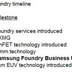
Samsung Foundry recently held their 4th annual technology forum in Santa Clara. This article reviews the highlights of the presentations. There were two prevalent themes throughout – focused execution on the current process roadmap, and the introduction of the 3nm process node features and schedule.
Before getting into … Read More
One of the interesting rumors in Taiwan last week was the possibility that UMC and GF will do a deal to merge or UMC will buy some GF fabs. I have talked to quite a few industry experts about it and will talk to more this week at the GSA US Executive Forum (more at the end). The US Executive Forum is what they call a C Level event which means it… Read More
Samsung Foundry recently held their annual technology forum in Santa Clara CA. The forum consisted of: presentations on advanced and mainstream process technology roadmaps; the IP readiness for those technology nodes; a review of several unique package offerings; and, an informal panel discussion with IP designers and EDA… Read More
There is an interesting discussion in the SemiWiki forum about EDA and the foundry business model which got me to thinking about the next disruptive move for the semiconductor industry. First let’s look at some of the other disruptive EDA events that I experienced firsthand throughout my 30+ year career.
When I started in 1984 EDA… Read More
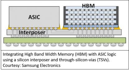
High Bandwidth Memory (HBM) systems have been successfully used for some time now in the network switching and high-performance computing (HPC) spaces. Now, adding fuel to the HBM fire, there is another market that shares similar system requirements as HPC and that is Artificial Intelligence (AI), especially AI systems doing… Read More
This week Dr. Eric Esteve, Dr. Bernard Murphy, and I will be blogging live from Arm TechCon. It really looks like it will be a great conference so you should see some interesting blogs in the coming days. One of the topics I am interested in this year is foundation IP and I will tell you why.
During the fabless transformation of the semiconductor… Read More
A significant shift is underway in the fabless semiconductor business model. As the application markets have become more diverse (and more cost-sensitive), product requirements have necessitated a new focus on multi-die packaging technology. … Read More
If you’re headed to #53DAC (June 5-9 in Austin,TX) and are interested in learning more about FD-SOI, there will be lots of opportunities. Here’s a quick guide to get you started. … Read More
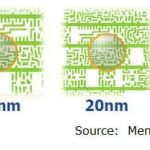
It is truly amazing to consider the advances in microelectronic process development, using 193i photolithography. The figure below is a stark reminder of the difference between the illuminating wavelength and the final imaged geometries. This technology evolution has been enabled by continued investment in mask data generation… Read More
Samsung Foundry had an intimate gathering recently for 200 customers and partners that I missed, but I know several people who attended. This event was a precursor to #53DAC where Samsung has the largest foundry presence. I was able to clarify what I had heard via a phone call with Kelvin Low so here is my version of what is important:… Read More