You are currently viewing SemiWiki as a guest which gives you limited access to the site. To view blog comments and experience other SemiWiki features you must be a registered member. Registration is fast, simple, and absolutely free so please,
join our community today!
Do we ever imagine what kind of severe challenges mission critical unmanned systems in air, land and underwater face? They are limited in space and size; have to be light in weight, flexible in different types of operations and at the same time rugged enough to work in extreme climatic conditions. That’s not enough; amidst these … Read More
With multiple functionalities added into a single chip, be it a SoC or an ASIC, maintaining low power consumption has become critical for any design. Various techniques at the technology as well as design level are employed to accomplish the low power target. These include thinner oxides in transistors, different sections of … Read More
Here, I am talking about reliability of chip design in the context of electrical effects, not external factors like cosmic rays. So, the electrical factors that could affect reliability of chips could be excessive power dissipation, noise, EM (Electromigration), ESD (Electrostatic Discharge), substrate noise coupling and… Read More
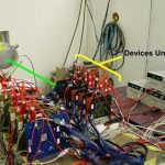
There are two ways to see how resistant your designs are to single-event errors (SEE). One is to take the chip or even the entire system and put it in a neutron beam and measure how many problems occur in this extreme environment. While that may be a necessary part of qualification in some very high reliability situations, it is also … Read More
At the onset of SoCs with multiple functionalities being packed together at the helm of technologies to improve upon performance and area; power, which was earlier neglected, has become critical and needs special attention in designing SoCs. And there comes reliability considerations as well due to multiple electrical and … Read More
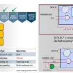
How reliable is your cell-phone? Actually, you don’t really care. It will crash from time to time due to software bugs and you’ll throw it away after two or three years. If a few phones also crash due to stray neutrons from outer space or stray alpha particles from the solder balls used in the flip-chip bonding then nobody… Read More
What do nVidia, Freescale and GlobalFoundries have in common? They are semiconductor companies? They are ARM licensees? They are doing 28nm chips? They all have the letter ‘a’ in their names?
All true, but that’s not what I was thinking of. But the letter ‘a’ is a clue since Apache (and Ansys) begin with ‘a’. All three companies have… Read More
Auto makers have historically been accused of things like planned obsolescence – redesigning parts to make repairs painfully or even prohibitively expensive – and the “warranty time-bomb”, where major systems seem to fail about a week after the warranty expires. Optimists would chalk both those up to relentless innovation,… Read More
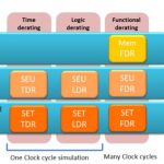
I blogged recently about reliability testing with high energy neutron beams. This is good for getting basic reliability data but it is not really a useful tool for worrying about reliability while the chip is still being designed and something can be done about it.
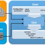
That is where IROC Technologies SOCFIT tool comes in. It takes all… Read More
So you want to know how reliable your chips are and how susceptible they are to single event effects (SEEs) where a neutron or an alpha particle causes a storage element (flop or memory cell) to flip in a way that alters the behavior of the device. There are two ways a particle hitting a device might not cause a problem. Firstly, the particle… Read More