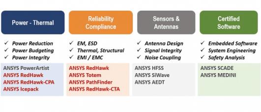
Power integrity and reliability are just as important for AMS designs as they are for digital designs. Ansys is offering a series of five webinars on this topic, under a heading they call ANSYS in ACTION, a bi-weekly demo series from ANSYS in which an application engineer shows you how simulation can address common applications.… Read More
Tag: reliability
Reliability Signoff for FinFET Designs
Ansys recently hosted a webinar on reliability signoff for FinFET-based designs, spanning thermal, EM, ESD, EMC and aging effects. I doubt you’re going to easily find a more comprehensive coverage of reliability impact and analysis solutions. If you care about reliability in FinFET designs, you might want to check out this webinar.… Read More
Webinar: Signoff for Thermal, Reliability and More in Advanced FinFET designs
In automotive applications, advanced FinFET processes are great for high levels of integration and low power. But they also present some new challenges in reliability signoff. Ansys will be hosting a webinar to highlight the challenges faced by engineers trying to ensure thermal, electromigration (EM) and electrostatic discharge… Read More
Simulating ADAS
Simulation is a broad technique spanning certainly digital logic and circuit simulation but also methods beyond these which are particularly relevant to ADAS design. In fact, much of the design of full ADAS systems begins and ends with these types of modeling. This is in part due to the need fully validate integrity and reliability… Read More
The Importance of EM, IR and Thermal Analysis for IC Design – Webinar
Designing an IC has both a logical and physical aspect to it, so while the logic in your next chip may be bug-free and meet the spec, how do you know if the physical layout will be reliable in terms of EM (electro-migration), IR (voltage drops) and thermal issues? EDA software once again comes to our rescue to perform the specific type… Read More
NVIDIA looks inside Parker and automotive-grade
‘Parker’ is a fascinating name for a chip designed for autonomous vehicles – more likely, the project name was pulled off a map as a bedroom community near Denver. First highlighted on the roadmap in 2013, and advertised as inside the DRIVE PX 2 platform shown at CES 2016, NVIDIA revealed some details of Parker at Hot Chips 2016.… Read More
Pushing automotive-grade embedded flash to 28nm
18 months ago Renesas announced they were prototyping their SG-MONOS eFlash on 28nm, and at the time we said it would be a couple of years before actual product. Yesterday, Renesas revealed their partner in this effort is TSMC – no surprise – and hinted things are moving, with better performance than expected but on a longer qualification… Read More
Six Reasons to Rethink Power Semiconductor Packaging
In my 40 years’ experience in power semiconductors I have visited thousands of customers, big and small, on every continent except Antarctica. When the issue invariably turns to the packaging of the power semiconductor – transistor, diode, or integrated circuit – the requests for improvement fall into six categories:
… Read More
3 reasons why diode-based ESD protection ruins the IoT experience
The ‘Dual diode’ approach is one of the most used on-chip and off-chip concept for ESD protection of IO interfaces. It is simple to implement, smaller than any other IO/ESD concept, has a low parasitic capacitance and low leakage.… Read More
Testing IGBTs before they go into EVs
In the pages of SemiWiki, we are usually talking about what to do with billions of really small transistors – for a change of pace today, we’ll discuss what to do with a few really big ones. Mentor Graphics has just announced their latest MicReD platform for thermal testing of IGBTs, experiencing a resurgence (pun intended) thanks… Read More


