You are currently viewing SemiWiki as a guest which gives you limited access to the site. To view blog comments and experience other SemiWiki features you must be a registered member. Registration is fast, simple, and absolutely free so please,
join our community today!
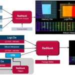
As we move towards packing more and more functionalities and increasing densities of SoCs, the power, thermal and signal integrity issues keep on rising. 3D-IC is a great concept to stack multiple dies on top of each other vertically. While it brings lot of avenues to package dies with multiple functions together, it has challenges… Read More
I think by now there has been good level of discussion on FinFET technology at sub-20 nm process nodes and this is an answer to ultra dense, high performance, low power, and billion+ gate SoC designs within the same area. However, it comes with some of the key challenges with respect to power, noise and reliability of the design. A FinFET… Read More
Since power has become a critical factor in semiconductor chip design, the stress is towards decreasing supply voltage to reduce power consumption. However, the threshold voltage to switch devices cannot go down beyond a certain limit and these results in an extremely narrow margin for noise between the two. And that gets further… Read More
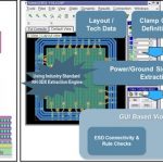
In this age of electronics, especially with so many different types of human held devices and more upcoming wearable devices, it’s utmost important to protect the massive circuitry inside those tiny parts in the devices from ESD related failures. The protection needs to happen at all stages – cells inside the chips, package… Read More
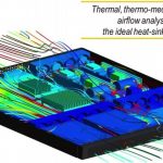
Last week my daughter was playing some games on my Google Nexus smartphone for a while when one of my friends called. When I picked up the phone, I couldn’t imagine it was so hot. There is no doubt; every electronic device today emits an order of magnitude higher heat than what it used to at most a decade ago. There is so much emphasis on … Read More
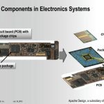
In today’s era of low power and high performance components, preferably on a single chip provides impetus to much larger electronic systems packaged into much smaller cases; smartphones are the immediate examples which encapsulate multiple functions other than the intended ones, viz. phone and data communication. As an example,… Read More
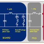
In July Cadence acquired Sigrity, one of the leaders in PCB and IC packaging analysis. Until a decade ago, signal integrity and power analysis was something that only IC designers needed to worry about. For all except the highest performance boards, relatively simple tools were sufficient. Provided you hooked up the pins on all… Read More
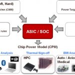
Aveek Sarkar presented a webinar on chip-package-system (CPS) earlier this summer. One of the big challenges with low-power electronic systems is that the performance, power and price goals are mutually conflicting. It’s like the old joke about “pick any 2”. But for a real system all need to be optimized. … Read More
Increasingly the challenge with SoCs, especially for mobile, is not getting the performance high enough but doing so in a power-efficient manner. Handheld devices running multiple apps need high-speed processors that consume extremely low levels of power both in operating and standby modes. In the server farm, the limit is … Read More
The webinar on CPS (chip-package-system) is on Tuesday 9th August at 11am Pacific time. It will be conducted by Christopher Ortiz, Principal Application Engineer at Apache Design Solutions. Dr. Ortiz has been with Apache since 2007, supporting the Sentinel product line. Prior to Apache he worked at Agere / LSI, where he investigated… Read More