TechInsights has been in the semiconductor analysis business for more than 35 years and is THE most trusted source of semiconductor information. TechInsights started as a reverse engineering and IP analysis company but has grown into much more. I remember waiting for the teardown reports before buying electronics to make sure… Read More
Tag: ic knowledge
SMIC N+2 in Huawei Mate Pro 60
Up until last December I was president and owner of IC Knowledge LLC, at the end of November, I sold IC Knowledge LLC to TechInsights. It has been interesting to become an insider at the world’s leading semiconductor reverse engineering and knowledge company. The latest SMIC N+2 analysis is an excellent example of TechInsight’s… Read More
SISPAD – Cost Simulations to Enable PPAC Aware Technology Development
I was invited to give a plenary address at the SISPAD conference in September 2021. For anyone not familiar with SISPAD it is a premiere TCAD conference. This year for the first time SISPAD wanted to address cost and my talk was “Cost Simulations to Enable PPAC Aware Technology Development”.
For many years the standard in technology… Read More
TSMC and Samsung 5nm Comparison
Samsung and TSMC have both made recent disclosures about their 5nm process and I though it would be a good time to look at what we know about them and compare the two processes.
A lot of what has been announced about 5nm is in comparison to 7nm so we will first review 7nm.
7nm
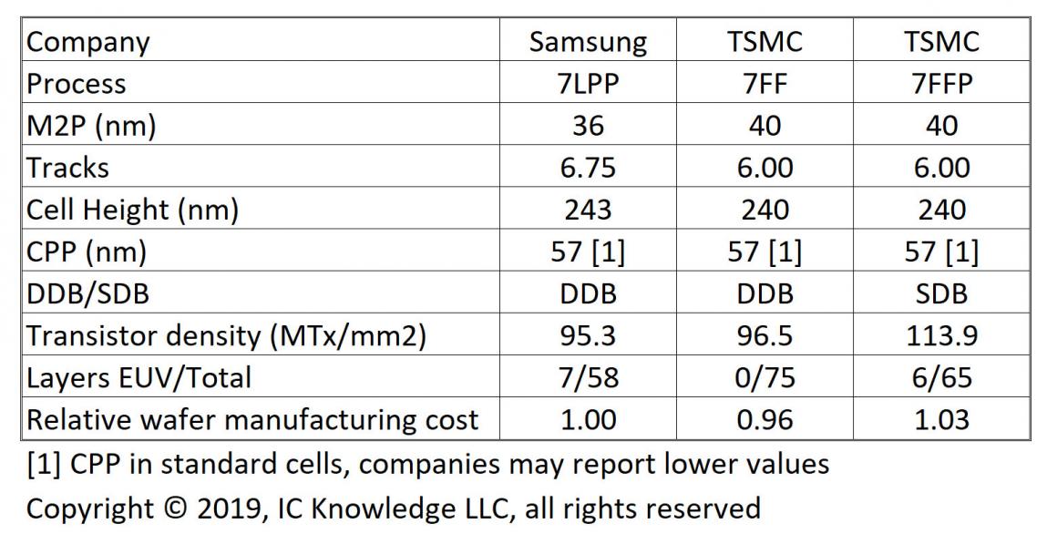
Figure 1 compares Samsung’s 7LPP process to TSMC’s 7FF and 7FFP… Read More
Samsung vs TSMC 7nm Update
The semiconductor foundry business has gone through a dynamic transformation over the last 30 years. In the beginning the foundries were several process nodes behind the IDMs with little hope of catching up. Today the foundries are leading the process development race at 10nm – 7nm, and will continue to do so, absolutely.… Read More
Samsung is Starting 7nm Production with EUV in June
There is a report in the Seoul Economic Daily that Samsung has completed development of their 7nm process using EUV and that production will begin in June. What is claimed in the report is:
- The process is installed in the Hwaseong S3 Fab
- Samsung has more than 10 EUV systems installed
- Production starts in June with Qualcomm, Xilinx,
IEDM 2017 Preview
The 63rd annual IEDM (International Electron Devices Meeting) will be held December 2nd through 6th in San Francisco. In my opinion IEDM is one of, if not the premier conference on leading edge semiconductor technology. I will be attending the conference again this year and providing coverage for SemiWiki. As a member of the press… Read More
3D NAND Myths and Realities
For many year 2D NAND drove lithography for the semiconductor industry with the smallest printed dimensions and yearly shrinks. As 2D NAND shrunk down to the mid-teens nodes, 16nm, 15nm and even 14nm, the cells became so small that there were only a few electrons in each cell and cross-talk issues made further shrinks very difficult… Read More
An Steegen ISS Talk and Interview – Patterning Options for Advanced Nodes
At the ISS Conference in January, An Steegen EVP of Semiconductor Technology & Systems at imec gave a talk entitled “Patterning Options for Advanced Technology Nodes”. I was present for her talk and had the opportunity to have a follow up interview with An.… Read More
Cost Modeling as a Decision Making Tool
The use of simulation is well established in the semiconductor industry. Virtually all circuit designs are run through a Spice simulation, layouts are analyzed for timing issues and even process development employs process simulation tools. What I believe is less widely used but just as useful is cost modeling.
The semiconductor… Read More


