You are currently viewing SemiWiki as a guest which gives you limited access to the site. To view blog comments and experience other SemiWiki features you must be a registered member. Registration is fast, simple, and absolutely free so please,
join our community today!
Whether EUV or DUV doesn’t matter at 20 nm pitch
The International Roadmap for Devices and Systems, 2022 Edition, indicates that the “2nm” node due in 2025 (this year) has a minimum (metal) half-pitch of 10 nm [1]. This is, in fact, less than the resolution of a current state-of-the-art EUV system, with a numerical aperture… Read More
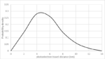
The occurrences of notorious stochastic defects in EUV lithography have resulted in CD or corresponding dose windows with the lower and higher bounds being characterized as “cliffs” [1-3], since the defect density increases exponentially when approaching these bounds. The defects at lower doses have been attributed to the… Read More
Conventionally, the resolution limit of a lithography system with wavelength l and numerical aperture NA is given by half-pitch = 0.25 wavelength/NA. With the use of EUV lithography, however, electron blur needs to be added [1]. The impact of this blur is to reduce the contrast [2]. Blur reduces the modulation amplitude by a factor… Read More
Previously, I had indicated how detrimental stochastic effects at pitches below 50 nm should lead to reconsidering the practical resolution limit for EUV lithography [1]. This is no exaggeration, as stochastic effects have been observed for 24 nm half-pitch several years ago [2,3]. This then leads to the question of whether … Read More
The latest significant development in EUV lithography technology is the arrival of High-NA systems. Theoretically, by increasing the numerical aperture, or NA, from 0.33 to 0.55, the absolute minimum half-pitch is reduced by 40%, from 10 nm to 6 nm. However, for EUV systems, we need to recognize that the EUV light (consisting … Read More
There has been much interest in Huawei’s and SMIC’s plans for 5nm production in the near future. Since there is no use of EUV in China, immersion DUV lithography (with a 76 nm pitch resolution) is expected to be used along with pitch quartering to achieve pitches in the 20-30 nm range expected for the 5nm and 3nm nodes [1].… Read More
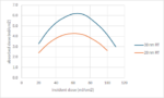
Resist blur remains a topic that is relatively unexplored in lithography. Blur has the effect of reducing the difference between the maximum and minimum doses in the local region containing the feature. Blur is particularly important for EUV lithography since EUV lithography is prone to stochastic fluctuations and also driven… Read More
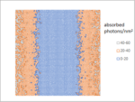
The majority of EUV production is on 5nm and 3nm node, implemented by late 2022. Metal oxide resists have not been brought into volume production yet [1,2], meaning that only organic chemically amplified resists (CARs) have been used instead until now. These resists have a typical absorption coefficient of 5/um [3,4], which means
…
Read More
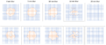
The discussion of any particular lithographic application often refers to imaging a single pitch, e.g., 30 nm pitch for a 5nm-family track metal scenario. However, it is always necessary to confirm the selected patterning techniques on the actual use case. The 7nm, 5nm, or 3nm 6-track cell has four minimum pitch tracks, flanked… Read More
On a DRAM chip, the patterning of features outside the cell array can be just as challenging as those within the array itself. While the array contains features which are the most densely packed, at least they are regularly arranged. On the other hand, outside the array, the regularity is lost, but the in the most difficult cases, … Read More