In the modern world, the semiconductor industry stands at the heart of technological innovation. From smartphones and laptops to advanced medical devices and artificial intelligence systems, nearly every piece of contemporary electronics depends on increasingly sophisticated microchips. Among the leading companies … Read More
Tag: finfets
CEO Interview with Scott Bibaud of Atomera
Scott Bibaud has served as President, Chief Executive Officer and a director since October 2015. Mr. Bibaud has been active in the semiconductor industry for over 25 years. He has successfully built a number of businesses in his career which grew to generate over $1 Billion in revenue at some of the world’s largest semiconductor… Read More
How the Father of FinFETs Helped Save Moore’s Law
In the early 2000s, Moore’s Law—the observation that the number of transistors on a chip doubles roughly every two years—was facing an existential crisis. As semiconductor nodes shrank below 90nm, planar transistors suffered from debilitating issues: leakage currents soared, power efficiency plummeted, and scaling became… Read More
Mastering Atomic Precision – ALD’s Role in Semiconductor Advancements
Atomic layer deposition (ALD) is a thin-film deposition method that continues to enable continuous advances in semiconductor device fabrication. Essentially, it involves exposing substrates sequentially to at least two different vapor phase atmospheres in which self-limiting reactions take place on the surface: the first… Read More
How Intel Stumbled: A Perspective from the Trenches
Bloomberg did an interview with my favorite semiconductor analyst Stacy Rasgon on “How the Number One U.S. Semiconductor Company Stumbled” that I found interesting. Coupled with the Q&A Bob Swan did at the Credit Suisse Annual Technology Conference I thought it would be good content for a viral blog.
Imec Technology Forum and ASML
On Thursday July 9 Imec held a virtual technology forum. Imec is one of the premier research organizations working on semiconductor technology and their forums are always interesting. My area of interest is process technology and the following are my observation in that area from the forum.
Luc Van Den Hove
Luc Van Den Hove is the… Read More
Online Class: Advanced CMOS Technology 2020 (The 10/7/5 NM Nodes)
Our friends at Threshold Systems have a new ONLINE class that may be of interest to you. It’s an updated version of the Advanced CMOS Technology class held last February. This is normally a classroom affair but to accommodate the recent COVID-19 travel restrictions it is being offered virtually.
As part of the previous class we did… Read More
A Quick TSMC 2019 Tech Symposium Overview
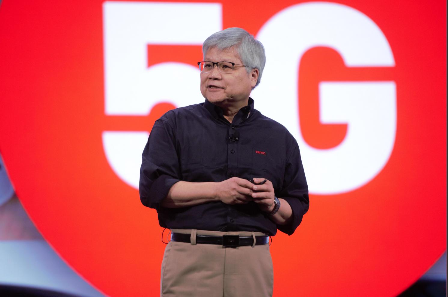
This year TSMC did a FinFET victory lap with the success of 16nm, 12nm, 10nm, and 7nm. It really is well deserved. Even though TSMC credits the ecosystem and customers, I credit TSMC and their relationship with Apple since it has pushed us all much harder than ever before. TSMC CEO C.C. Wei summed it up nicely in his keynote: Innovation,… Read More
IEDM 2018 Trip Report!
Hello, my name is Daniel Nenni and I am a semiconductor conference addict. I just can’t seem to get enough. The semiconductor ecosystem is very wide now and moves so quickly it is nearly impossible to keep up without constant conference attendance. As a SemiWiki contributor not only do I get free conference passes, I get access to … Read More
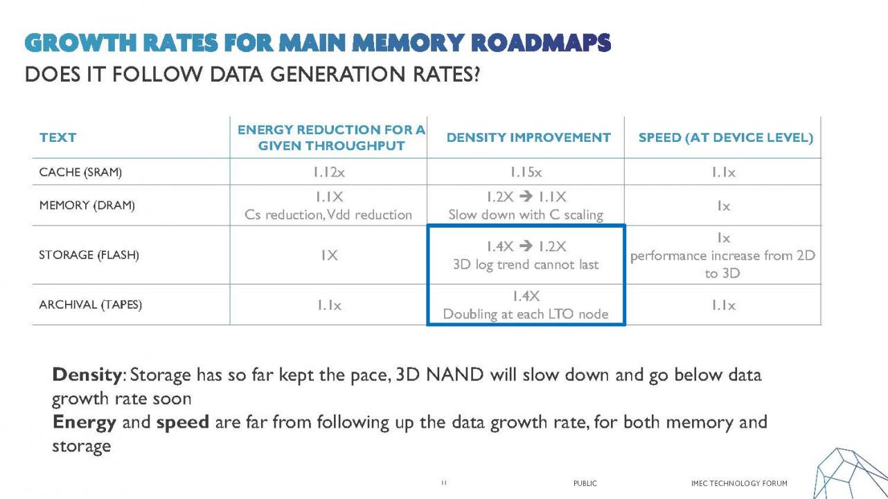
Imec technology forum 2018 – the future of memory
At the Imec technology forum in Belgium Gouri Sankar Kar and Arnaud Furnemont presented memory and storage perspectives and I also got to interview Arnaud. Arnaud leads overall memory development at Imec and personally leads NAND and DNA research.
Memory research is focused on power, energy, speed and cost with energy and throughput… Read More


