You are currently viewing SemiWiki as a guest which gives you limited access to the site. To view blog comments and experience other SemiWiki features you must be a registered member. Registration is fast, simple, and absolutely free so please,
join our community today!
If you are ever asked to organize a conference session do not hesitate, accept immediately and jump right in. When John Swan, EDPS General Chair, asked me to organize a day I hesitated. Fortunately he is not one to take no for an answer. It was an unforgettable experience on many levels and I hope to be involved with EDPS again next year.… Read More
The 20th annual Electronic Design Process Symposium (EDPS) held April 18-19 at the Monterey Beach Hotel in Monterey California was an unqualified success. I know this because a bird (seagull?) sitting on the window sill of the conference room was so captivated by the fascinating insight provided by a number of luminaries that … Read More
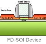
I recently spoke to Arvind Narayanan, Product Marketing Manager for Mentor’s place and route division about emerging technology. This of course led to FinFETS, FDSOI, performance, power, and cost-benefit. The battle between FDSOI and FinFETs, said Narayanan, is going to be something to watch.
Both FDSOI and FinFET technologies… Read More
This year’s recipient of the Kaufman Award is Dr Chenming Hu. I can’t think of a more deserving recipient. He is the father of the FinFET transistor which is clearly the most revolutionary thing to come along in semiconductor for a long time. Of course he wasn’t working alone but he was the leader of the team at UC… Read More
Cliff Hou of TSMC gave the keynote today at SNUG on Collaborate to Innovate: a Foundry’s Perspective. Starting around 45nm the way that a foundry has to work with its ecosystem fundamentally changed. Up until then, each process generation was similar enough to the previous one, apart obviously from size, that it could be … Read More
Synopsys ♥ FinFETsby Daniel Nenni on 03-03-2013 at 6:00 pmCategories: EDA, Synopsys
FinFETs are fun! They certainly have kept me busy writing over the past year about the possibilities and probabilities of a disruptive technology that will dramatically change the semiconductor ecosystem. Now that 14nm silicon is making the rounds I will be able to start writing about the realities of FinFETs which is very exciting!… Read More
At DAC 2012 we were hearing about the 20nm design ecosystem viability, however IC process technology never stands still so we have early process development going on now at the 10nm and 14nm nodes where FinFET technology is being touted. Earlier in February Vassilios Gerousis, a distinguished engineer at Cadence presented a session… Read More
The fabless revolution in the digital semiconductor industry is no more, with just a few integrated device manufacturers (IDMs) remaining on the playing field, it is now the normal way to do business. However, the learning curve for each new process node continues as it always has, with a host of new technical challenges for the … Read More
One of the privilages of blogging for SemiWiki is invitations to the top conferences around the world including the International Solid-State Circuits Conference (ISSCC) in San Francisco this week. Amazing, this conference is older than I am:
ISSCC 2013 is the 60th Conference in an incredibly long-lasting series. Following… Read More
Tubes of the Futureby Paul McLellan on 02-07-2013 at 10:00 pmCategories: General
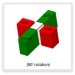
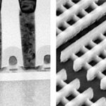
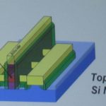
So what is a silicon nanowire? It is basically a FET where the active element is a wire 3-20nm in diameter. So where a FinFET has the gate wrapped around 3 sides of the transistor, a nanowire (NW) has it wrapped around all four. In essence, the wire runs through the middle of the gate.
There seem to be three issues about building a silicon… Read More