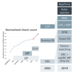
EUV lithography systems continue to be the source of much hope for continuing the pace of increasing device density on wafers per Moore’s Law. Recently, although EUV systems were originally supposed to help the industry avoid much multipatterning, it has not turned out to be the case [1,2]. The main surprise has been the
Tag: euv
Revisiting EUV Lithography: Post-Blur Stochastic Distributions
In previous articles, I had looked at EUV stochastic behavior [1-2], primarily in terms of the low photon density resulting in shot noise, described by the Poisson distribution [3]. The role of blur to help combat the randomness of EUV photon absorption and secondary electron generation and migration was also recently considered… Read More
KLAC- Foundry/Logic Drives Outperformance- No Supply Chain Woes- Nice Beat
KLA- great quarter driven by continued strong foundry/logic
No supply chain hiccups- Riding high in the cycle
Wafer inspection remains driver with rest along for the ride
Financials remain best in industry
A superb quarter
There was little to complain about in the quarter. Revenues of $2.1B and EPS of $4.64, both nicely beating… Read More
The Challenge of Working with EUV Doses
Recently, a patent application from TSMC [1] revealed target EUV doses used in the range of 30-45 mJ/cm2. However, it was also acknowledged in the same application that such doses were too low to prevent defects and roughness. Recent studies [2,3] have shown that by considering photon density along with blur, the associated shot… Read More
Blur, not Wavelength, Determines Resolution at Advanced Nodes
Lithography has been the driving force for shrinking feature sizes for decades, and the most easily identified factor behind this trend is the reduction of wavelength. G-line (436 nm wavelength) was used for 0.5 um in the late 1980s [1], and I-line (365 nm wavelength) was used down to 0.3 um in the 1990s [2]. Then began the era of deep-ultraviolet… Read More
Cautions In Using High-NA EUV
High-NA EUV has received a lot of attention ever since Intel put the spotlight on its receiving the first 0.55 NA EUV tool from ASML [1], expected in 2025. EUV itself has numerous issues which have been enumerated by myself and others, most notoriously the stochastic defects issue. There are also a host of issues related to the propagation… Read More
KLA – Chip process control outgrowing fabrication tools as capacity needs grow
-KLA dominates process control like ASML dominates litho
-Industry in “panic mode” over capacity drives process control
-Like others, KLA tool supplies are in demand & tight supply
-Balance of 2021 “filled out” – now booking for 2022
Solid numbers and very solid guide for a better second … Read More
EDA in the Cloud – Now More Than Ever
A decade ago, many of us heard commentaries on how entrepreneurs were turned down by venture capitalists for not including a cloud strategy in their business plan, no matter what the core business was. Humorous punchlines such as, “It’s cloudy without any clouds” and “Add some cloud to your strategy and your future will be bright… Read More
ASML- A Semiconductor Market Leader-Strong Demand Across all Products/Markets
– Strong demand across logic/memory & leading/trailing edge
– Customers want units fast-no time to test
– The main question is can ASML ramp to meet demand?
Revenue & Earnings low due to systems being rushed to customers
ASML reported Euro 4B in sales and Euro 1B in net income which while within guidance… Read More
Stochastic Origins of EUV Feature Edge Roughness
Due to the higher energy of EUV (13.3-13.7 nm wavelength) compared to ArF (193 nm wavelength) light, images produced by EUV are more susceptible to photon shot noise.
Figure 1. (Left) 40 nm dense (half-pitch) line image projected onto wafer at 35 mJ/cm2; (Right) 20 nm dense (half-pitch) line image projected onto wafer at 70 mJ/cm2.… Read More


