You are currently viewing SemiWiki as a guest which gives you limited access to the site. To view blog comments and experience other SemiWiki features you must be a registered member. Registration is fast, simple, and absolutely free so please,
join our community today!
A Brief History of Mentor Graphicsby Beth Martin on 08-20-2012 at 11:00 pmCategories: EDA, Siemens EDA
In 1981, Pac-Man was sweeping the nation, the first space shuttle launched, and a small group of engineers in Oregon started not only a new company (Mentor Graphics), but an entirely new industry, electronic design automation (EDA).
Mentor founders Tom Bruggere, Gerry Langeler, and Dave Moffenbeier left Tektronix with a great… Read More
Big processors get all the love, it seems. It’s natural, since they are highly complex beasts and need a lot of care and feeding in the EDA and fab cycle. But the law of large numbers is starting to shift energy in the direction of optimizing microcontrollers.
I mulled the math in my head for a while. In a world with 7 billion people and … Read More
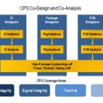
One of the really big changes about chip design is the way over the last decade or so it is no longer possible to design an SoC, a package for it to go in and the board for the package using different sets of tools and methodologies and then finally bond out the chip and solder it onto the board. The three systems, Chip-Package-System have… Read More
There was a day, not too long ago, when a software developer could be intimate with a processor through understanding its register set. Before coding, developers would reach for a manual, digging through pages and pages of 1s and 0s with defined functions to find how to gain control over the processor and its capability. One bit set… Read More
A Brief History of EDAby Daniel Nenni on 08-05-2012 at 6:00 pmCategories: EDA
Electronic Design Automation, or more affectionately known as EDA, is a relatively young $5B industry with a very colorful upbringing, one that I have experienced firsthand, I’m very grateful for, and is an honor to write about. Today EDA employs an estimated 27,000 people! There is a nice EDA Wikipedia page which can be found here… Read More
Today it was announced that Synopsys is acquiring SpringSoft for $406 million dollars ($12.2B Taiwanese). Coincidentally, I was in SpringSoft’s US office yesterday to talk about how Laker is being used for 20nm design. More of that later. But there was certainly nothing to indicate that anyone there was expecting this.… Read More
Cadence has a series of webinars about their digital flow, focused on 28nm design. It is easy for all of us in the EDA ecosystem to assume that everyone is already doing 20/22nm design, if not 14nm already. But in fact most designs are still being done at 45nm and 65nm; 28nm is still a big challenging step.
One of the tools in the Cadence… Read More
Josefina Hobbs, a solutions architect at Synopsys, shows the integration of Synopsys Protocol Analyzer with SpringSoft’s Verdi using the Verdi Interoperability Apps (VIA) which gives open access to the Verdi KDB and FSDB databases. She also demonstrates protocol debug made easy using the Protocol Analyzer. This gives… Read More
About 4 years ago some of my semiconductor cohorts urged me to blog. “Hey Dan, you’re a funny guy, write about EDA and IP, make us laugh!” Of course what I think is funny most people think is snarky, which is a nice word for being a smart ass. The traditional semiconductor press was crumbling, the non traditional EDA websites were outdated,… Read More


