You are currently viewing SemiWiki as a guest which gives you limited access to the site. To view blog comments and experience other SemiWiki features you must be a registered member. Registration is fast, simple, and absolutely free so please,
join our community today!
I sat down last week for lunch with Michael Sanie. Mike and I go back a long way, working together at VLSI Technology (where his first job out of school was to take over the circuit extractor that I’d originally written) and then in strategic marketing at Cadence. Now Mike has marketing for (almost?) all of Synopsys’s … Read More
Over at the GSA Forum website I have an article on the history of the semiconductor industry. It is actually based on a couple of brief history of semiconductor blogs (here and here) I published here on SemiWiki last year but edited down a lot and tightened up.
Since the start of the year seems to be the time for predictions, here are the… Read More
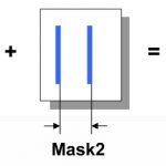
TSMC and Synopsys hosted a webinar in December on this topic of double patterning and how it impacts the IC extraction flow. The 20nm process node has IC layout geometries so closely spaced that the traditional optical-based lithography cannot be used, instead lower layers like Poly and Metal 1 require a new approach of using two… Read More
This is the second blog entry about an ST Ericsson white-paper on multiprocessors in mobile. The first part was here.
The first part of the white-paper basically shows that for mobile the optimal number of cores is two. It is much better to use process technology (and good EDA) to run the processor at higher frequency rather than add… Read More
We will soon start to see the quarterly financial reporting installments of the “Big 3” public EDA companies. I predict they will be as boring as usual. I am not sure if I would want it any differently though.
Back in the 90s there were times when it was truly interesting to wait to see what Cadence, Mentor, or later Synopsys, might announce.… Read More
Oasys Has a New CEOby Paul McLellan on 01-18-2013 at 2:21 pmCategories: EDA
Scott Seaton is the new CEO of Oasys Design Systems. Paul van Besouw, the CEO since the company’s founding, becomes the CTO. I met Scott last year when I was doing some consulting work for Carbon Design where he was VP of sales (the new VP sales at Carbon is Hal Conklin, by the way).
I talked to Scott about why he had joined Oasys. … Read More
David Avercrombie of Mentor won the award for the best tutorial at the 2012 TSMC OIP for his presentation, along with Peter Hsu of TSMC, on Finding and Fixing Double Patterning Errors in 20nm. The whole presentation along with the slides is now available online here. The first part of the presentation is an introduction to double … Read More
Apache Design Solutions was founded in 2001 by Andrew Yang and three researchers from HP Labs (Norman Chang, Shen Lin, Weize Xie). They realized that engineers striving to meet the goal of increased device miniaturization, as defined by Moore’s Law, would eventually hit stumbling blocks in their progress. The founding team believed… Read More
I’ve taught Verilog classes and used logic synthesis tools for ASIC and FPGA designs, so was interested to hear about Oasys Design Systems. I attended their webinar at 9AM today, so I’ll share what I learned about their approach to logical and physical synthesis. This approach competes with tools like Design Compiler… Read More
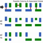
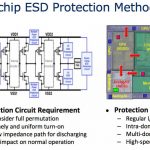
In Pune at the start of the month, Norman Chang, Ting-Sheng Ku, Jai Pollayil of Apache/Ansys and NVIDIA presented and ESD check methodologywith Fast Full-chip Static and Macro-level Dynamic Solutions . ESD stands for Elecro-Static Discharge and is basically injecting very high static voltages (think how your hand gets charged… Read More