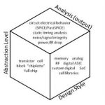
Memory Cell Characterization with a Fast 3D Field Solver

Memory Cell Characterization with a Fast 3D Field Solver
by Daniel Payne on 09-29-2011 at 12:07 pm

Memory designers need to predict the timing, current and power of their designs with high accuracy before tape-out to ensure that all the design goals will be met. Extracting the parasitic values from the IC layout and then running circuit simulation is a trusted methodology however the accuracy of the results ultimately depend… Read More


Aug 25th in Fremont, CA – Hands on Calibre workshop: DRC, LVS, xRC, ERC, DFM

Aug 25th in Fremont, CA – Hands on Calibre workshop: DRC, LVS, xRC, ERC, DFM
by Daniel Payne on 08-18-2011 at 10:30 am

I’ve blogged about the Calibre family of IC design tools before:

Smart Fill replaced Dummy Fill Approach in a DFM Flow
DRC Wiki
Graphical DRC vs Text-based DRC
Getting Real time Calibre DRC Results with Custom IC Editing
Transistor-level Electrical Rule Checking
Who Needs a 3D Field Solver for IC Design?
Prevention is BetterRead More


August 11th – Hands-on Workshop with Calibre: DRC, LVS, DFM, xRC, ERC

August 11th – Hands-on Workshop with Calibre: DRC, LVS, DFM, xRC, ERC
by Daniel Payne on 08-06-2011 at 9:29 pm

I’ve blogged about the Calibre family of IC design tools before:

Smart Fill replaced Dummy Fill Approach in a DFM Flow
DRC Wiki
Graphical DRC vs Text-based DRC
Getting Real time Calibre DRC Results with Custom IC Editing
Transistor-level Electrical Rule Checking
Who Needs a 3D Field Solver for IC Design?
Prevention is BetterRead More


Smart Fill Replaces Dummy Fill Approach in a DFM Flow

Smart Fill Replaces Dummy Fill Approach in a DFM Flow
by Daniel Payne on 07-30-2011 at 7:11 pm

I met with Jeff Wilson, Product Marketing Manager at Mentor in the Calibre product group to learn more about Smart Fill versus Dummy Fill for DFM flows. Jeff works in the Wilsonville, Oregon office and we first meet at Silicon Compilers back in the 1990’s.

Dummy Fill

This diagram shows an IC layout layer on the left as originallyRead More


Graphical DRC vs Text-based DRC

Graphical DRC vs Text-based DRC
by Daniel Payne on 05-01-2011 at 11:42 am

Introduction
IC designs go through a layout process and then a verification of that layout to determine if the layout layer width and spacing rules conform to a set of manufacturing design rules. Adhering to the layout rules will ensure that your chip has acceptable yields.

At the 28nm node a typical DRC (Design Rule Check) deck will… Read More


Who Needs a 3D Field Solver for IC Design?

Who Needs a 3D Field Solver for IC Design?
by Daniel Payne on 04-07-2011 at 4:53 pm

Inroduction
In the early days we made paper plots of an IC layout then measured the width and length of interconnect segments with a ruler to add up all of the squares, then multiplied by the resistance per square. It was tedious, error prone and took way too much time, but we were rewarded with accurate parasitic values for our SPICE… Read More


DRC/DFM inside of Place and Route

DRC/DFM inside of Place and Route
by Daniel Payne on 03-31-2011 at 10:19 am

Intro
Earlier this month I drove to Mentor Graphics in Wilsonville, Oregon and spoke with Michael Buehler-Garcia, Director of Marketing and Nancy Nguyen, TME, both part of the Calibre Design to Silicon Division. I’m a big fan of correct-by-construction thinking in EDA tools and what they had to say immediately caught my… Read More


Getting Real Time Calibre DRC Results

Getting Real Time Calibre DRC Results
by Daniel Payne on 03-10-2011 at 10:00 am

Last week I met with Joseph Davis, Ph.D. at Mentor Graphics in Wilsonville, Oregon to learn about a new product designed for full-custom IC layout designers to improve productivity.

The traditional flow for full-custom IC layout designers has been nearly unchanged for decades:

  • Read a schematic or use Schematic Driven Layout
Read More

New ERC Tools Catch Design Errors

New ERC Tools Catch Design Errors
by glforte on 02-11-2011 at 2:18 pm

388 image001

A growing number of reports highlight a class of design errors that is difficult to check using more traditional methods, and can potentially affect a wide range of IC designs, especially where high reliability is a must.By Matthew Hogan

Today’s IC designs are complex. They contain vast arrays of features and functionality in Read More


Computational Lithography, Scaling’s Best Friend

Computational Lithography, Scaling’s Best Friend
by glforte on 11-03-2010 at 11:51 pm

attachment

By Joseph Sawicki, Vice President & General Manager, Design to Silicon Division

It is one of the more amazing stories in the continued march of Moore’s Law over the past four nodes. Previously scaling was enabled solely though changes in the physical domain, whether through decreasing the wavelength of light, increasing … Read More