Inroduction
In the early days we made paper plots of an IC layout then measured the width and length of interconnect segments with a ruler to add up all of the squares, then multiplied by the resistance per square. It was tedious, error prone and took way too much time, but we were rewarded with accurate parasitic values for our SPICE circuit simulations.
Today we have many automated technologies to choose from when it comes to extracting parasitic values for an IC layout. These parasitic values ensure that what we simulate in SPICE is accurately providing the right timing value, can detect glitches and measure the effects of cross-talk.
Accuracy vs Speed
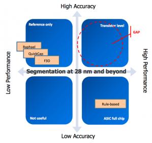
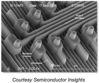
The first automated parasitic extraction tools used rules about each interconnect layer for resistance and capacitance as a function of width, length and proximity to other layers. These tools are fast and reasonable accurate for nodes that have wide interconnect with little height. As the height of interconnect have grown then the accuracy of these rules diminishes because of the complex 3D nature of nearby layers.
3D field solvers have been around for over a decade and have also offered the ultimate in accuracy with the major downside being slow run times. The chart above places 3D field solvers in the upper left hand corner, high accuracy and low performance.
Here’s a quick comparison of four different approaches to extracting IC parasitics:
[TABLE] class=”cms_table_grid”
|- class=”cms_table_grid_tr”
| class=”cms_table_grid_td” | Approach
| class=”cms_table_grid_td” | Plus
| class=”cms_table_grid_td” | Minus
|- class=”cms_table_grid_tr”
| class=”cms_table_grid_td” | Rule-based/Pattern Matching
| class=”cms_table_grid_td” | Status quo
Familiar
Full-chip
| class=”cms_table_grid_td” | Unsuitable for complex structures
Unable to reach within 5% of reference
|- class=”cms_table_grid_tr”
| class=”cms_table_grid_td” | Traditional Field Solver
| class=”cms_table_grid_td” | Reference Accuracy
| class=”cms_table_grid_td” | Long run times
Limited to devices
|- class=”cms_table_grid_tr”
| class=”cms_table_grid_td” | Random-Walk Field Solver
| class=”cms_table_grid_td” | Improved Integration
| class=”cms_table_grid_td” | 3 to 4X slower than Deterministic
|- class=”cms_table_grid_tr”
| class=”cms_table_grid_td” | Deterministic Field Solver
| class=”cms_table_grid_td” | Reference-Like Accuracy
Fast as Rule-based
| class=”cms_table_grid_td” | Multi-cpu required (4 – 8)
|-
What if you could find a tool that was in the upper right hand corner, offering high accuracy and fast run times?
That corner is the goal of a new breed of 3D field solvers where highest accuracy and fast run times co-exist.
Mentor’s 3D Field Solver
 I learned more about 3D field solvers from Claudia Relyea, TME at Mentor for the Calibre xACT 3D tool, when we met last month in Wilsonville, Oregon. The xACT 3D tool is a deterministic 3D field solver where multiple CPUs are used to achieve faster run times. A white paper is available for download here.
Q: Why shouldn’t I try a 3D field solver with a random-walk approach?
A: Well, your results with a random-walk tool will have a higher error level. Let’s say that you have 1 million nets in your design, then with a sigma of 1% you will see 3,000 nets where the accuracy is >3% different from a reference result. For sensitive analog circuits and data converters that level of inaccuracy will make your chip fail.
Q: What is the speed difference between xACT 3D and random walk tools?
A: We see xACT 3D running about 4X faster.
Q: What kind of run times can I expect with your 3D field solver?
A: About 120K nets/hour when using 32 cpus, and 65K nets/hour with 16 cpus.
Q: How is the accuracy of your tool compared to something like Raphael?
A: On a 28nm NAND chip we saw xACT 3D numbers that were between 1.5% and -2.9% of Raphael results.
Q: Which customers are using xACT 3D?
A: Over a dozen, the one’s that we can mention are: STARC, eSlicon and UMC.
Q: For a device level example, how do you compare to a reference field solver?
A: xACT 3D ran in 9 seconds versus 4.5 hours, and the error versus reference was between 4.5% and -3.8%.
Q: What kind of accuracy would I expect on an SRAM cell?
A: We ran an SRAM design and found xACT 3D was within 2.07% of reference results.
Q: How does the run time scale with the transistor count?
A: Calibre xACT 3D has linear run time performance with transistor count. Traditional field solvers have an exponential run time with transistor count making them useful for only small cells.
Q: What is the performance on a large design?
A: A memory array with 2 million nets runs in just 28 hours when using 16 cpus.
Q: Can your tool extract inductors?
A: Yes, it’s just an option you can choose.
Q: How would xACT 3D work in a Cadence IC tool flow?
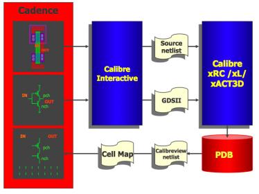
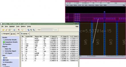
Q: Can I cross-probe parasitics in Cadence Virtuoso?
A: Yes, that uses Calibre RVE.
Q: Where would I use this tool in my flow?
A: Every place that you need the highest accuracy: device, cell and chip levels.
Summary
3D field solvers are not just for device level IC parasitics, in fact they can be used on cell and chip level as well when using multiple CPUs. The deterministic approach by Mentor gives me a safer feeling than the random-walk method because I don’t need to worry about accuracy.
I’ve organized a panel discussion at DAC on the topic of 3D field solvers, so hope to see you in San Diego this June.


Comments
0 Replies to “Who Needs a 3D Field Solver for IC Design?”
You must register or log in to view/post comments.