You are currently viewing SemiWiki as a guest which gives you limited access to the site. To view blog comments and experience other SemiWiki features you must be a registered member. Registration is fast, simple, and absolutely free so please,
join our community today!
Introducing on-chip test circuitry has become a necessary criteria for an ASIC’s post manufacture testability. The test circuitry is usually referred as DFT (Design-for-Test) circuit. A typical methodology for introducing DFT circuit in a design is to replace usual flip-flops with special types of flip-flops called ‘scan… Read More
In a semiconductor design, keeping the design testable with high test coverage has always been a requirement. However with shrinking technology nodes and large, dense SoC designs and complex logic structures, while it has become mandatory to reach close to 100% test coverage, it’s extremely difficult to cope with the explosion… Read More
What’s next in test compression?by Beth Martin on 10-10-2014 at 4:45 pmCategories: Events, Siemens EDA
If you’ll be at ITC TestWeek in Seattle (Oct 20-23), here’s one event you don’t want to miss: a technology reception hosted by Mentor, with Janusz Rajski and Nilanjan Mukherjee as the featured speakers. It is free to ITC attendees and you can register here. [If for some crazy reason you haven’t registered for ITC yet, do that… Read More
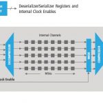
With advancement of semiconductor technologies, ever increasing sizes of SoCs bank on higher densities of design rather than giving any leeway towards increasing chip area and package sizes; a phenomenon often overlooked. The result is – larger designs with lesser number of pins bonded out of ever shrinking package sizes;… Read More
Test engineers are often the unsung heroes in the semiconductor world, because they have the tough job of deciding if each IC is good or bad, while taking the least amount of time on a tester and ensuring that the tests are actually finding and uncovering all manufacturing and process variation defects. Simple stuck-at fault models… Read More
While focus of the semiconductor industry has shifted to DACin this week and unfortunately I couldn’t attend due to some of my management exams, in my spare time I was browsing through some of the webpages of Cadenceto check their new offerings (although they have a great list of items to showcase at DAC) and to my pleasure I came across… Read More
With the advent of large SoCs in semiconductor design space, verification of SoCs has become extremely challenging; no single approach works. And when the size of an SoC can grow to billions of gates, the traditional methods of testability of chips may no longer remain viable considering the needs of large ATPG, memory footprint,… Read More
3D-IC has a stack of dies connected and packaged together, and therefore needs new testing strategies other than testing a single die. It’s given that a single defective die can render the whole of 3D-IC unusable, so each die in the stack must be completely and perfectly tested before its entry into that stack. Looking at it from a … Read More
Traditional logic testing relies on blasting pattern after pattern at the inputs, trying to exercise combinations to shake faults out of logic and hopefully have them manifested at an observable pin, be it a test point or a final output stage. It’s a remarkably inefficient process with a lot of randomness and luck involved.
Getting… Read More
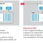
Traditionally ATPG (Automatic Test Pattern Generation) and BIST (Built-In-Self-Test) are the two approaches for testing the whole semiconductor design squeezed on an IC; ATPG requires external test equipment and test vectors to test targeted faults, BIST circuit is implemented on chip along with the functional logic of IC.… Read More