You are currently viewing SemiWiki as a guest which gives you limited access to the site. To view blog comments and experience other SemiWiki features you must be a registered member. Registration is fast, simple, and absolutely free so please,
join our community today!
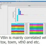
Analog IP is more difficult to design and optimize for a given process node compared to digital IP, so any automation for analog designers is always welcome. The engineers at SMIC in China have customers that design analog IP and often they need to know how to optimize it for a specific process, so I watched a presentation by Josh Yang,… Read More
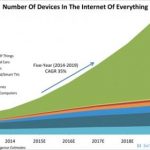
The semiconductor industry is expected to grow at a reasonable pace in 2015 and beyond, with the biggest market being compute applications followed by wireless and consumer applications. The highest growth, however, is expected to be in application-specific products for devices such as smartphones, wearables, memories, … Read More
In a world where Application Specific Integrated Circuits (ASICs) and Application Specific Standard Products (ASSPs) are dominating every conceivable application, greater attention is being applied to their long term reliability. These chips are being built on smaller lithographies, running at higher speeds, dissipating… Read More
Most analog cells have a power off mode intended to reduce power consumption. In this mode, all the circuit branches between the supply lines are set in a high impedance mode by driving MOS gates to a blocking voltage. This is a somewhat similar situation to that in tri-state digital circuits.
When a branch is set in that high impedance… Read More
Designing an SoC requires a team, and the engineers typically use lots of specialized EDA software and semiconductor IP to get the job done. Many have started to ask about how designing a chip is different than designing and managing a large software project, or how is analog design different than digital design in terms of managing… Read More
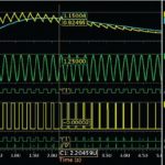
Workshops are a great where to learn hands-on about IC design technology. Mentor has a free workshop to introduce you to creating, simulating and verifying mixed-signal (Analog and Digital) designs.
PLL waveforms showing both digital and analog signals.
Dates in Fremont, California
July 26, 2011
September 15, 2011
November… Read More