You are currently viewing SemiWiki as a guest which gives you limited access to the site. To view blog comments and experience other SemiWiki features you must be a registered member. Registration is fast, simple, and absolutely free so please,
join our community today!
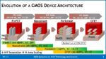
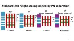
The 2020 VLSI Technology Symposium was held as a virtual conference from June 14th through June 19th. At the symposium Imec gave an interesting paper on Monolithic CFET and I had a chance to interview one of the authors, Hiroaki Arimura.
It is well known in the industry that FinFETs (FF) are reaching the end of their scaling life. Samsung… Read More
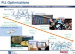
TSMC’s Open Innovation Platform’s main objective is to create and promote partnership for producing chips. This year’s OIP event included a presentation on the joint efforts of Silicon Creations, Mentor, a Siemens business and TSMC to produce essential PLL IP for 5nm and 3nm designs. The relentless push for smaller geometries… Read More
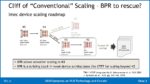
The 2020 VLSI Technology Symposium was held as a virtual conference from June 14th through June 19th. At the symposium Imec gave an interesting paper on Buried Power Rails (BPR) and I had a chance to interview one of the authors, Anshul Gupta.
As logic devices continue to scale down metal pitch is reaching a limit. Imec defines a pitch… Read More
On May 15th TSMC “announced its intention to build and operate an advanced semiconductor fab in the United States with the mutual understanding and commitment to support from the U.S. federal government and the State of Arizona.”
The fab will run TSMC’s 5nm technology and have a capacity of 20,000 wafers per month (wpm). Construction… Read More
Recently Seeking Alpha published an article “Taiwan Semiconductor Manufacturing Company Losing Its Process Leadership To Intel” and Dan Nenni (SemiWiki founder) asked me to take a look at the article and do my own analysis. This is a subject I have followed and published on for many years.
Before I dig into specific process density… Read More
I couldn’t attend the SPIE Advanced Lithography Conference this year for personal reasons, but last week Mike Lercel of ASML was nice enough to walk me through the major ASML presentations from the conference.
Introduction
In late 2018, Samsung and TSMC introduced 7nm foundry logic processes with 5 to 7 EUV layers, throughout … Read More
Imec is one of the premier semiconductor research organizations and at IEDM they presented dozens of papers. I had the opportunity to see several of the papers presented and interview 3 of Imec’s researchers.
Jan Van Houdt, DMTS ferroelectric and exploratory memory
I have had very interesting discussions with Imec researchers… Read More
On Tuesday night of IEDM, Applied Materials held a panel discussion “The Future of Logic: EUV is Here, Now What?”. The panelists were: Regina Freed, managing director at Applied Materials as the moderator, Geoffrey Yeap, senior director of advanced technology at TSMC, Bala Haran, director of silicon process research at IBM, … Read More
The IEEE International Electron Devices Meeting is in my opinion the leading technology conference to understand the current state-of-the-art in semiconductor process technology. Held each year in early December in San Francisco it is a must attend conference for anyone following technology development. The following is… Read More
On Monday, July 8th Imec held a technology forum ahead of Semicon West. I saw the papers presented and interviewed three of the authors. The following is a summary of what I feel are the keys points of their research.
Arnaud Furnemont
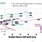
Arnaud Furnemont’s talk was titled “From Technology Scaling to System Optimization”. Simple 2D … Read More