You are currently viewing SemiWiki as a guest which gives you limited access to the site. To view blog comments and experience other SemiWiki features you must be a registered member. Registration is fast, simple, and absolutely free so please,
join our community today!
At the 2021 Symposium on VLSI Technology and Circuits in June a short course was held on “Advanced Process and Devices Technology Toward 2nm-CMOS and Emerging Memory”. In this article I will review the first two presentations covering leading edge logic devices. The two presentations are complementary and provide and excellent… Read More
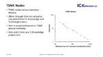
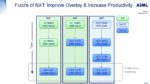
Recently, TSMC held their annual Technology Symposium, providing an update on the silicon process technology and packaging roadmap. This article will review the highlights of the silicon process developments and future release plans.
Subsequent articles will describe the packaging offerings and delve into technology … Read More
Over the recent years, the volume and velocity of discussions relating to chiplets have intensified. A major reason for this is the projected market opportunity. According to research firm Omdia, chiplets driven market is expected to be $6B by 2024 from just $645M in 2018. That’s an impressive nine-fold projected increase over… Read More
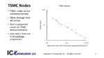
IBM has announced the development of a 2nm process.
IBM Announcement
What was announced:
- “2nm”
- 50 billion transistors in a “thumbnail” sized area later disclosed to be 150mm2 = 333 million transistors per millimeter (MTx/mm2).
- 44nm Contacted Poly Pitch (CPP) with 12nm gate length.
- Gate All Around (GAA), there are several ways
…
Read More
TSMC recently announced plans to spend $100 billion dollars over three years on capital. For 2021 they announced $30B in total capital with 80% on advanced nodes (7nm and smaller), 10% on packaging and masks and 10% on “specialty”.
If we take a guess at the capital for each year, we can project something like $30B for 2021 (announced),… Read More
In January I presented at the ISS conference a comparison of Intel’s, Samsung’s and TSMC’s leading edge offerings. You can read a write-up of my presentation here.
With the problems going on at Intel, that article generated a lot of interest in the investment community, and I have been holding a lot of calls with analysts who are trying… Read More
At the SPIE Advanced Lithography Conference held in February, ASML presented the latest information on their Deep Ultraviolet (DUV) and Extreme Ultraviolet (EUV) exposure systems. I recently got to interview Mike Lercel of ASML to discuss the presentations.
DUV
Despite all the attention EUV is getting, most layers are still… Read More
There are reports in the media that TSMC is now planning six Fabs in Arizona (the image above is Fab 18 in Taiwan). The original post I saw referred to a Megafab and claimed six fabs with 100,000 wafers per month of capacity (wpm) for $35 billion dollars. The report further claimed it would be larger than TSMC fabs in Taiwan.
This report… Read More
There is a lot of interest right now in how Intel compares to the leading foundries and what the future may hold.
Several years ago, I published several extremely popular articles converting processes from various companies to “Equivalent Nodes” (EN). Nodes were at one time based on actual physical features of processes but had… Read More
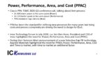
I was asked to give a talk at the 2021 ISS conference and the following is a write up of the talk.
The title of the talk is “Logic Leadership in the PPAC era”.
The talk is broken up into three main sections:
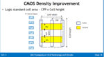
- Background information explaining PPAC and Standard Cells.
- A node-by-node comparisons of companies running leading edge logic
…
Read More