You are currently viewing SemiWiki as a guest which gives you limited access to the site. To view blog comments and experience other SemiWiki features you must be a registered member. Registration is fast, simple, and absolutely free so please,
join our community today!
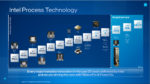
Last Thursday Intel held their investors meeting, in this write up I wanted to focus on my areas of coverage/expertise, process technology and manufacturing.
Technology Development presented by Ann Kelleher
Last year Intel presented their Intel Accelerated plan and, in this meeting, we got a review of where Intel stands on that… Read More
Kinam Kim is a longtime Samsung technologist who has published many excellent articles over the years. He is now the Chairman of Samsung Electronics, and he gave a very interesting keynote address at IEDM.
He began with some general observations:
The world is experiencing a transformation powered by semiconductors that has been… Read More
IBM at IEDMby Scotten Jones on 01-10-2022 at 6:00 amCategories: Events
IBM transferred their semiconductor manufacturing to GLOBALFOUNDRIES several years ago but still maintains a multibillion-dollar research facility at Albany Nanotech. IBM is very active at conferences such as IEDM and appears to have a good public relations department because they get a lot of press.
At the Litho Workshop … Read More
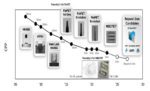
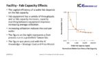
The incredible growth that the semiconductor industry has enjoyed over the last several decades is attributed to Moore’s Law. While no one argues that point, there is also industry wide acknowledgment that Moore’s Law started slowing down around the 7nm process node. While die-size reductions still scale, performance jumps… Read More
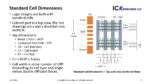
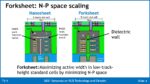
Standard Cell Scaling
Complex logic designs are built up from standard cells, in order to continue to scale logic we need to continually shrink the size of standard cells.
Figure 1 illustrates the dimensions of a standard cell.
Figure 1. Standard Cell Dimensions.
From figure 1 we can see that shrinking standard cell sizes requires… Read More
I was invited to give a plenary address at the SISPAD conference in September 2021. For anyone not familiar with SISPAD it is a premiere TCAD conference. This year for the first time SISPAD wanted to address cost and my talk was “Cost Simulations to Enable PPAC Aware Technology Development”.
For many years the standard in technology… Read More
Anyone who has read my previous articles about IEDM knows I consider it the premier conference on process technology.
Last year due to COVID IEDM was virtual and although virtual offers some advantages the hallway conversations that can be such an important part of the conference are lost. This year IEDM is returning as a live event… Read More
The big fake news last week came from a report out of China stating that TSMC won a big Intel order for 3nm wafers. We have been talking about this for some time on SemiWiki so this is nothing new. Unfortunately, the article mentioned wafer and delivery date estimates that are unconfirmed and from what I know, completely out of line. … Read More
Intel presented yesterday on their plans for process technology and packaging over the next several years. This was the most detailed roadmap Intel has ever laid out. In this write up I will analyze Intel’s process announcement and how they match up with their competitors.
10nm Super Fin (SF)
10nm is now in volume production in three… Read More
FinFETs devices are reaching their limits for scaling. Horizontal Nanosheets (HNS) are a type of Gate All Around (GAA) device that offers better scaling and performance per unit area. HNS is the logical next step from FinFETs because HNS processing is similar to FinFETs with a limited number of process changes required.
At the … Read More