You are currently viewing SemiWiki as a guest which gives you limited access to the site. To view blog comments and experience other SemiWiki features you must be a registered member. Registration is fast, simple, and absolutely free so please,
join our community today!
EDPS: 3D ICs, part Iby Paul McLellan on 04-10-2012 at 10:00 pmCategories: EDA, Events
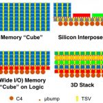
The second day (more like a half-day) of EDPS was devoted to 3D ICs. There was a lot of information, too much to summarize in a few hundred words. The keynote was by Riko Radojcic of Qualcomm, who has been a sort of one-man-band attempting to drive the EDA and manufacturing industries towards 3D. Of course it helps if you don’t … Read More
And no red and green glasses required.
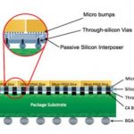
I remember the first time I heard about a Through Silicon Via (TSV), punching a hole through the entire wafer to make an electrical connection at the back, like we do all the time in printed circuit boards with through plated holes. I thought someone was trying one on and trying to make me look a fool.… Read More
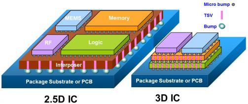
In my last article I talked about the physical design aspect of 3D-IC. Now looking at its verification aspect, it spans through a wide spectrum of test at hardware as well as software level. The verification challenge goes much beyond that of a SoC which is at a single plane. Even a typical SoC that comprises of a processor core, memory… Read More
EDPS Montereyby Paul McLellan on 03-17-2012 at 8:00 amCategories: EDA, Events
Every year in Monterey is a relatively small conference that looks at the design process, EDPS, the electronic design process symposium. I gave a keynote there a couple of years ago, but you don’t have to listen to me this time. The keynotes are from:
- 1st day: Misha Buric, CTO of Altera, talking about SoC FPGAs and other things
…
Read More
As I have been watching the developments in EDA and Semiconductor industry, it is apparent that we remain fragmented unless pushed to adopt a common standard mostly due to business reasons. Foundries are dictating on the rules to be followed by designs, thereby EDA tools incorporating them. Also, design companies needed to work… Read More
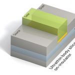
The 1999 IDM paper Sub 50-nm FinFET: PMOSstarted the 3D transistor ball rolling, then in May of 2011 Intel announceda production version of a 3D transistor (TriGate) technology at 22nm. Intel is the leader in semiconductor process technologies so you can be sure that others will follow. Intel has a nice “History of the Transistor… Read More
When process nodes reached 28 nm and below, it appeared that design density is reaching a saturation point, hitting the limits of Moore’s law. I was of the opinion that the future of microelectronic physical design was limited to 20 and 14 nm being addressed by technological advances such as FinFETs, double patterning, HKMG (High-k… Read More
The ASIC business is getting more and more complicated. The ability to produce innovative die at a competitive price to solve increasingly complex problems just isn’t enough. The technology required to package that die is now front and center.
Here, at the junction of advanced design, process technology and state-of-the art … Read More
Looking at the huge gap between the revenue of semiconductor design and manufacturing (~$300B) and that of EDA tools, services and silicon IP combined (~6B) inspired me to look more deeply into the overall arena of semiconductors in today’s context and possibly decipher some trends which should emerge in near future. Although… Read More
The IEEE has an Orange Country Chapter of the Components, Packaging and Manufacturing Technology Society who are organizing an all-day workshop, 3D Integrated Circuits: Technologies Enabling the Revolution. This looks to be an informative day with real-world examples in both design and test being presented by over a dozen … Read More