One of the greatest hockey players of all time, Wayne Gretzky, provided a quote that has also been applied to the business world — “I skate to where the puck will be, not to where it has been.” It strikes me that this philosophy directly applies to IP development, as well. Engineering firms providing IP must anticipate how customer requirements will evolve, and execute a design and qualification plan well in advance of the demand curve.
I recently had the opportunity to chat with members of the engineering team at Analog Bits, providers of IP for SerDes lanes, PLL’s, memories, on-chip sensors, and I/O’s for memory (and general purpose) interfaces. They impressed upon me characteristics of current development projects that are “critical success factors” to the IP business model:
- multi-protocol SerDes IP extends applicability across markets
Analog Bits has focused on development of SerDes IP to be applied for several serial interface protocols.
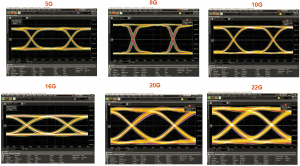
- IP providers must lead in the development of (standards for) next generation high-speed SerDes data rates.
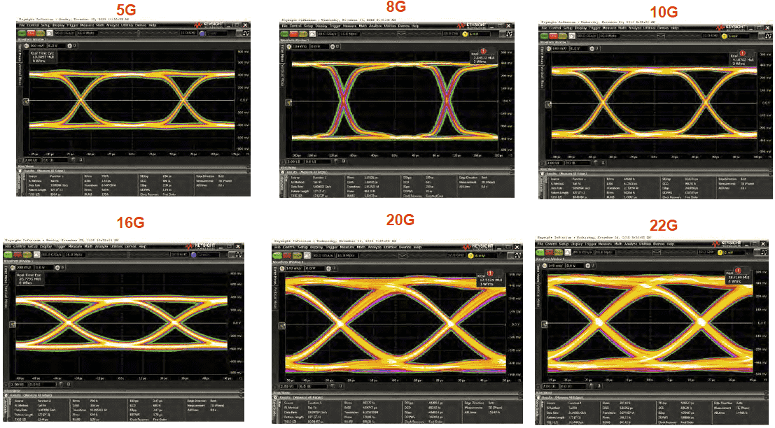
The silicon testsite plan at Analog Bits involves demonstration of 25G data rates (at leading process technology nodes).
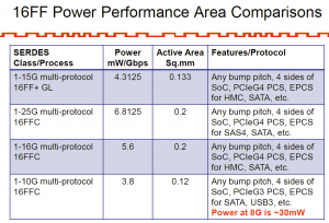
- Testsite silicon requires anticipating customer integration, test, and qualification requirements.
To be successful, testsite development requires a “skate to where the puck will be” strategy. Developing testsite shuttles is costly, both in NRE for silicon wafers and board-level testbench development and in engineering development resources. The IP team must invest wisely, to ensure that the resulting test measurement and qualification data will satisfy future customer requirements.
ESD qualification of I/O’s requires addressing the (evolving) CDM and HBM robustness standards demanded by end markets (e.g., JEDEC and AEC-Q100 tests).
SerDes IP on a testsite shuttle requires a test plan that demonstrates an adequate eye opening, using a topology representative of the losses that are likely to be present in the system design environment. The wrapback test specification used for IP evaluation is key — e.g., “total loss less than 22dB at 8GHz (for 16Gbps) through a loop back including 24″ of FR-4 trace”.
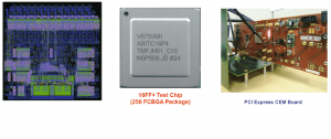
The SerDes physical (hard IP) implementation on the testsite also requires addressing future customer needs. The granularity of SerDes lanes, with the corresponding pad topology for signals and power, needs to satisfy a wide range of applications. The figure below illustrates the modular approach that Analog Bits has pursued.

Another example of engineering development to address customer requirements is the availability of SerDes IP cells for any die side of the customer’s SoC. At advanced process nodes, recall that an increasing number of mask layers must use unidirectional segments — e.g., device gates, lower-level metals. Unique IP cells are required for the different sites of the die. The figure below illustrates the vertical orientation SerDes cell on silicon testsites, and several examples of floorplanning testcases.
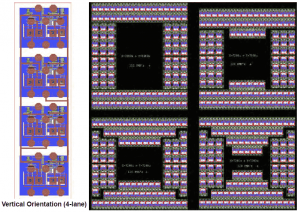
High-speed lanes are becoming more prevalent than other I/O types for performance-driven SoC’s. Demonstration of flexible, modular (hard) SerDes IP implementations with many lanes is a must.
The team at Analog Bits is focusing their engineering development and test resources on IP designs and shuttle testsites that anticipate the requirements of new markets for advanced process nodes. They are following the same approach that earned Gretzky the nickname “The Great One”.
For general information on the IP available from Analog Bits, please follow thislink.
-chipguy
Share this post via:


Comments
There are no comments yet.
You must register or log in to view/post comments.