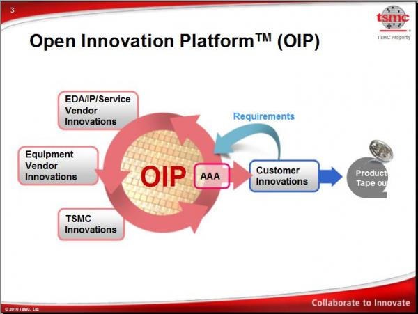
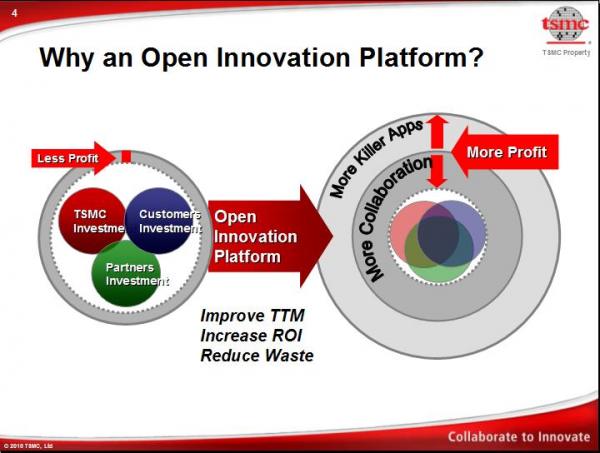
TSMC today extended one of the most effective semiconductor design enablement initiatives the semiconductor world has ever seen, the Open Innovation Platform (OIP). Morris Chang coined the term “OIP” himself in 2008, but the effort itself is 10+ years old with a collective cost > .5B$. My other blogs on topic include: TSMC OIP vs CDNS OIP Analysis, TSMC Open Innovation Platform Explained, andTSMC iPDK Debate.

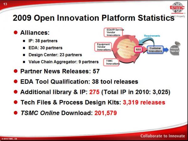
The Open Innovation Platform’s global EcosystemAllianceprograms have grown to include 30 EDA partners, 38 IP partners, 23DesignCenterAlliance(DCA) partners, and 9 Value Chain Aggregator (VCA) partners. All partners participate in one or more of the Open Innovation Platform collaboration programs. TSMC also begins to work collaboratively with industry organizations, such as IPL Alliance and Si2, to promote the interoperability standards based on TSMC interoperable EDA formats.
Impressive! But is TSMC the #1 semiconductor foundry because of their design enablement activities? Or is this design enablement initiative #1 because TSMC is the industry leading foundry?

I like the executive quotes included in the official TSMC press release, they speak volumes:
“The electronic design community is embracing the EDA360 vision to enable fastest approach from concept to consumer and together with IP suppliers, EDA vendors and silicon manufacturers, we have diligently collaborated to build a cohesive path for designers,” said Lip-Bu Tan, president and chief executive officer, Cadence. “TSMC’s Open Innovation Platform is a proven, integral part of this path. TSMC’s Open Innovation Platform will now make significant advancements in low-power, mixed-signal, system-level and 3D-IC design to enable further productivity improvements that our mutual customers need.”


News flash: The semiconductor community has NOT embraced EDA360. Just because you keep saying something over and over does not make it true, especially when it is self serving. I have spoken to dozens of semiconductor industry professionals and the foregone conclusion is that EDA360 is aNothing Burger!
“Going forward,Mentor and TSMC are developing complete solutions for the TSMC design ecosystem, ” said Walden C. Rhines, Chairman and CEO,Mentor Graphics. “The TSMC OIP effort is not just words — theMentor Track in Reference Flow 11.0, and the co-developed iDRC and iLVS languages, are real usable results.”


I like Wally’s style here, say more with less. My lunch with Wally is next week so hopefully I can get him to say more on the subject.
“Collaboration across the entire design eco-system — customers, foundries, IP and EDA suppliers — is critical for lower design risk and cost, better power and performance, and customer differentiation, ” said Aart de Geus, Chairman and CEO, Synopsys. “The new technologies in this phase of TSMC OIP, such as system-level design, analog/mixed-signal (AMS) design and thru-silicon-via, bring key solutions to speed System-to-IC realization.”


Aart is pointing out that the TSMC OIP not only competes directly with the Cadence EDA360 OIP, it plays to the strengths of Synopsys. In fact, the EDA360 Manifesto highlights the strengths of both Mentor and Synopsys: System Realization, SoC Realization, and Silicon Realization. Synopsys and Mentor own EDA360.


The most interesting quote, or lack there of, is from Magma CEO Rajeev Madhaven. Seriously, Magma is an integral part of the TSMC OIP expansion but no quote from Rajeev? I would like to think it is a conspiracy against Magma by the top 3 EDA CEO’s as a result of Magma’s business practices, but I’m sure there is a far less interesting explanation.


