The 17[SUP]th[/SUP] annual TSMC Technical Symposium finished its North American tour in Boston, a day before the Boston Marathon. I would like to be clever and say the foundry business is also a marathon but it clearly is not. If you watch TSMC, the foundry business is both a sprint AND a marathon!
In contrast to the previous blog on Global Foundries, the three key points to TSMC’s success are Leadership, Technology, and Experience. Rick Cassidy, President of TSMC North America, opened the symposiums with 30 slides of analogies and perspective featuring the US Olympic Bobsledding team.

Point #1 Leadership: Clearly TSMC is the leading foundry in all aspects of the business. The question is can TSMC continue in that role for another decade? I think the answer rests squarely on point #2.
Point #2 Technology: My 30 minute meeting with Dr. Shang-Yi Chiang, Vice President of TSMC R&D, should be a blog in itself but let me say here that he is one of the smartest, humble, and most believable men I have met. The big announcement Dr Chiang made was that TSMC would skip 22nm in favor of 20nm. My first question was why? Well, for two reasons (1) TSMC continues to see a 70% shrink as the optimum scaling factor: 40nm->28nm, 28nm->20nm, 20nm->14nm, 14nm-> 10nm. (2) Is my reason: Because TSMC can, and it gives them a competitive advantage. The predominate foundry business challenge is price cutting (2[SUP]nd[/SUP] and even 3[SUP]rd[/SUP] sourcing) so making your process as sticky as possible is the ultimate business goal. High volume designs will absolutely take advantage of the performance/power/area savings of a 20nm process versus 22nm. Look for the other foundries to follow suit as they did with 45 to 40nm in order to be competitive.
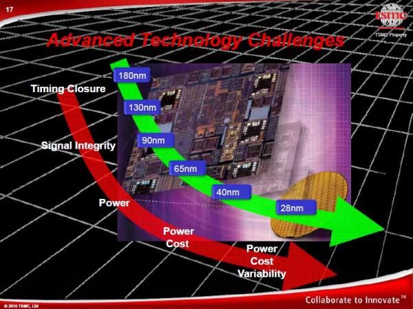
My second question for Dr Chiang was why Gate-Last versus Gate-First for 28nm? TSMC actually had parallel 28nm projects: Gate-First, Gate-Last, and Poly Gate. The winner was the Gate-Last 28nm implementation coupled with Restricted Design Rules due to scalability, performance, and yield. Dr Chang also stated that there is not an area penalty using RDRs which defies my personal experience with Recommend Design Rules.
My third question was about 40nm, what really happened with yield? Dr Chiang viewed it positively as a “learning” experience which resulted in technologies and practices that will enable 28nm and below (restricted design rules). TSMC saw 40nm designs with 4 billion + single VIAs, so VIA failure was an issue. Process variation was also a major issue, which I have blogged about before:
Moore’s Law and 28nm Yield
Moore’s Law and 40nm Yield
Dr Chaing did say that 40nm is “comfortably in production” at Fab 12 and 14. Expansion projects will double TSMC 40nm capacity by the end of the year. Giga Fabs like 12 and 14 can produce 100,000+ 12 inch wafers per month! Compared to Mini Fabs (10k+) and Mega Fabs (30k+). Capacity and the ability to satisfy the high volume needs of the top fabless semiconductor companies is key, believe it. He also said 28nm is on track with risk production in Q2 2010, which puts TSMC 6 months ahead of GlobalFoundries.
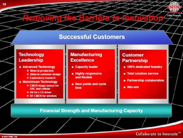
Point#3 Experience:TSMC also owns this one. IDM experience and Foundry experience are two very different things. One example is semiconductor IP and how it integrates into your design. Characterized, Modeled, Silicon proven IP from TSMC itself and TSMC early access partners like Virage Logic will ease integration issues and speed wafer sales. IP such as SRAM is used as pipe cleaners for new processes, which is why Virage was the first to announce products on TSMC 28nm. Other experience examples include silicon proven PDKs, Reference Design Kits and Flows.
This is my favorite Rick Cassidy slide, tight integration indeed:

My second favorite slide: mega fab costs are comparable to a Nimitz Class Aircraft carrier, minus the aircraft ($5B+). The question is, how many companies will be able to afford a fleet of aircraft carriers in the coming years, TSMC and?



Silicon Insurance: Why eFPGA is Cheaper Than a Respin — and Why It Matters in the Intel 18A Era