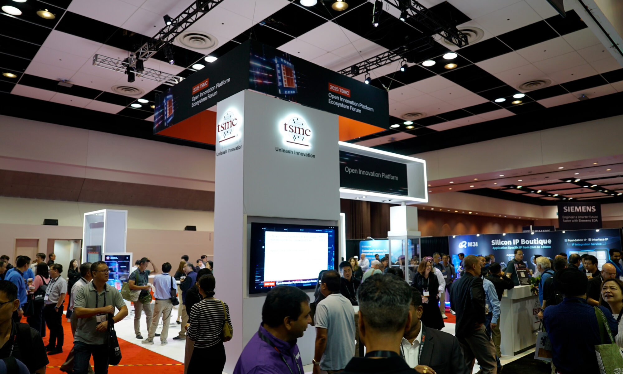


Now that the dust has settled let’s talk more about TSMC’s Open Innovation Platform. Launched in 2008, OIP represents a groundbreaking collaborative model in the semiconductor industry. Unlike IDMs that controlled the entire supply chain, OIP fosters an “open horizontal” ecosystem uniting TSMC with EDA providers, IP developers, cloud partners, design centers, and value chain players. This network, now spanning over 100 partners, has invested trillions of dollars cumulatively to align around TSMC’s technology roadmap, enabling faster innovation and specialization. As of 2025, OIP continues to evolve with recent expansions like the 3DFabric Alliance accelerating 3D IC advancements for AI and HPC.
The ecosystem’s core strength lies in its comprehensive alliances: EDA Alliance for certified tools, IP Alliance for silicon-verified blocks, Cloud Alliance for scalable design environments, Design Center Alliance (DCA) for expert services, Value Chain Alliance (VCA) for backend support, and specialized groups like 3DFabric for advanced packaging. These components lower barriers, ensuring “first-time silicon success” and driving shared value. Below, we break down the primary benefits for customers (chip designers), partners, and the broader industry.
1. Accelerated Design and Time-to-Market
OIP drastically shortens the path from concept to production, addressing the semiconductor industry’s relentless pace. By integrating TSMC’s process technologies with partner tools and IP, it reduces design cycle times by providing pre-validated interfaces and flows.
For instance:
- Cloud-Based Design: Through the Cloud Alliance (partners like AWS, Google Cloud, and Microsoft Azure), customers overcome in-house compute limits, enabling “design-in-the-cloud” for scalability and agility. This has cut time-to-market for complex chips by weeks to months.
- AI-Assisted Flows: At the 2024-2025 OIP Forums, ecosystem demos showcased AI-optimized 2D/3D IC designs, boosting productivity for AI and 5G applications.
- 3D Innovation: The 3DFabric Alliance, launched in 2022, speeds silicon stacking and chiplet integration, as seen in AMD’s TSMC-SoIC-based CPUs, which achieved energy-efficient HPC breakthroughs.
Statistics highlight the impact: OIP has enabled over 1,800 chip tape-outs, with partners like Silicon Creations contributing to 1,000+ advanced-node designs. Testimonials from Synopsys emphasize how OIP’s multi-die tools deliver “powerful and efficient processing” for hyperscale computing.
2. Cost Reduction and Efficiency Gains
OIP minimizes financial risks by democratizing access to premium resources, allowing smaller firms to compete with giants.
- Lower Barriers: Silicon-verified IP catalogs (the industry’s largest) and EDA certifications reduce R&D duplication, cutting development costs by up to 30-50% through reusable blocks like PLLs and SerDes.
- Shared Investments: Ecosystem collaborations, backed by billions in annual spending, spread costs across partners. For example, Siemens EDA Calibre 3DThermal integration with TSMC processes provides thermal analysis without custom tooling.
- Design Services: DCA and VCA offer outsourced expertise for testing and packaging, ideal for resource-constrained teams.
This efficiency has been pivotal for mobile and IoT innovations, where rapid prototyping via OIP’s Virtual Design Environment (launched 2018) avoids expensive iterations.
3. Enhanced Collaboration and Ecosystem Synergy
OIP’s “partner management portal” via TSMC-Online fosters seamless communication, turning competition into co-creation.
- Supply Chain Alignment: Standardized interfaces (e.g., 3Dblox for chiplet packaging) ensure interoperability, as noted by Siemens EDA: “OIP has been pivotal to advancing certified flows.”
- Global Forums: Annual events like the 2025 North America OIP Forum in Santa Clara unite 1,000+ attendees for multi-track sessions on AI, photonics, and RF, sparking real-time problem-solving.
- Award-Winning Partnerships: 2025 honorees like Teradyne (for 3DFabric testing) and Silicon Creations (ninth straight Mixed-Signal IP award) exemplify how OIP drives mutual growth, with TSMC’s Aveek Sarkar praising their role in “energy-efficient AI chip innovation.”
4. Industry-Wide Innovation and Scalability
Beyond individual gains, OIP propels the sector forward by supporting emerging tech like 2nm nodes, UCIe standards, and silicon photonics. It has nurtured innovations in automotive, 5G, and edge AI, with partners like imec contributing R&D for low-volume prototyping. The result? A resilient ecosystem that shortens “time-to-revenue” while promoting sustainability through efficient designs.
Bottom line: TSMC’s OIP transforms semiconductor development from siloed efforts to a vibrant, collaborative powerhouse. As AI demands surge, its benefits of speed, savings, synergy, and scalability position it as indispensable, empowering innovators to outpace Moore’s Law. For deeper dives, explore TSMC’s OIP page and the most recent forum recap: TSMC’s Push for Energy-Efficient AI: Innovations in Logic and Packaging.
Also Read:
Analog Bits Steps into the Spotlight at TSMC OIP
Synopsys Collaborates with TSMC to Enable Advanced 2D and 3D Design Solutions
Sofics’ ESD Innovations Power AI and Radiation-Hardened Breakthroughs on TSMC Platforms
Synopsys and TSMC Unite to Power the Future of AI and Multi-Die Innovation
Share this post via:


Comments
There are no comments yet.
You must register or log in to view/post comments.