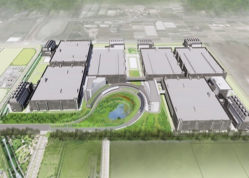
There are reports in the media that TSMC is now planning six Fabs in Arizona (the image above is Fab 18 in Taiwan). The original post I saw referred to a Megafab and claimed six fabs with 100,000 wafers per month of capacity (wpm) for $35 billion dollars. The report further claimed it would be larger than TSMC fabs in Taiwan.
This report struck me as not reliable given that TSMC refers to their large fab clusters as Gigafabs not Megafabs and TSMC’s Fab 12, Fab 14, and Fab 15 each have capacity of around 300,000 wpm and Fab 18 is ramping to over 200,000 wpm.
Now similar reports are being repeated in more reputable sources, notably today I saw a report in EE News Europe that stated:
- The site would be a Gigafab (correct terminology).
- Filings with the city of Phoenix describe three phases of building.
- TSMC has reportedly offered to double employee salaries to move to the US.
I am still not sure about the six fab part, the Phoenix documents are reported to say three phases although I suppose each phase could be two fabs. The other issue I have is that 100,000 wpm for six fabs is just under 17,000 wpm per fab, those are smaller fabs than TSMC typically builds and would be sub optimal from a cost perspective.
What I would think would be more likely is three fabs of just over 30,000 wpm each for a total of 100,000 wpm. Maybe they will build three fabs initially for 100,000 wpm and then have the option to build three more fabs later for an additional 100,000 wpm. Fab 18 in Taiwan has three fabs P1, P2 and P3 that are running 5nm with an original capacity of just under 30,000 wpm each although they are now being expanded to 40,000 wpm each, 120,000 wpm total. There is also P4, P5, and P6 under construction for 3nm that will likely each be around 30,000 wpm each initially bringing the site to around 200,000 wpm.
The $35 billion dollar price tag is high for 100,000 wpm of 5nm but would make sense if it also included some preparation for additional phases or 3nm capability. I should also point out the initial budget number for fabs is often an estimate and can increase or decrease as the fab is built depending on final capacity and how many fab phases are included in the initial amount. I believe TSMC has spent more money on phase 1, 2 and 3 of Fab 18 for 5nm than they originally announced and will also be spending more money on phases 4, 5 and 6 for 3nm than originally announced.
My best guess as of todays is the fab will have three phases initially producing 100,000 wpm total with the option to add three more phases in the futures to reach 200,000 wpm, that would be more consistent with TSMC Fab 18 in Taiwan.
However, the specifics work out it does appear that TSMC is now looking at building a full scale Gigafab in the US instead of the small fab originally planned. I see this as good news for the global semiconductor supply due to the high risk presented by having so much of the world’s leading edge logic capacity concentrated in Taiwan. This is especially concerning with Taiwan being located on an active fault line, the view in China that Taiwan is a rouge province that must be brought back under China control and the resource limits of a small island.
Share this post via:


Comments
9 Replies to “TSMC Plans Six Wafer Fabs in Arizona”
You must register or log in to view/post comments.