As I write this I sit heavyhearted in the EVA executive lounge returning from my 69[SUP]th[/SUP] trip to Taiwan. I go every month or so, you do the math. This trip was very disappointing as I can now confirm that just about everything you have read about TSMC 28nm yield is absolutely MANURE!
Please let me apologize to the hard working people of TSMC and the leading edge fabless semiconductor engineers that are bringing 28nm silicon to our hands and homes this year. On behalf of all of the people around the world who Blog and Tweet ignorant things, they know not what they type, I’m very very sorry.
Side bar: Even though you are not the origin of misinformation, Re-Tweeting is a legally actionable offense, especially if you are a self-proclaimed expert in the field. Don’t believe me? Check the “New Media” defamation case law that is now jamming the judicial systems around the world!
The problem with riding the TSMC 28nm yield defamation train is that at some point in time you will run out of track (you will be proven wrong), and that time is coming right around the bend, believe it.

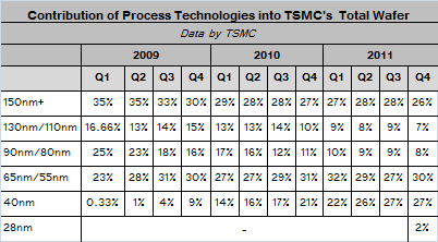
First, let’s look at the ramping history of the TSMC processes. This is public data made available to investors (TSMC is a publicly traded company, TSM – NYSE) so all SEC rules apply here. For reference, this is the first four quarters of production silicon based on percentage of wafer revenue:
65nm
[LIST=1]
40nm
[LIST=1]
28nm
[LIST=1]
As you can see, 40nm was a difficult ramp for a variety of reasons. 65nm was a much more typical ramp. Clearly the 28nm yield ramp, if it is as I predict, is very good so everybody who blogged, Tweeted or re-Tweeted otherwise is full of GUANO! And don’t you worry, I’m keeping a list.
The real TSMC 28nm issue is capacity and let me explain that as well. It normally takes 2-3 years and billions of dollars to build and ramp a semiconductor fab. TSMC recently did it in less than 2 years with Fab 15 but that was certainly not the norm three years ago. Now think back three years in regards to the economy. We were in the midst of the “Great Recession” scratching our heads wondering where our equity went. Literally, I’m half the man I was in 2007.

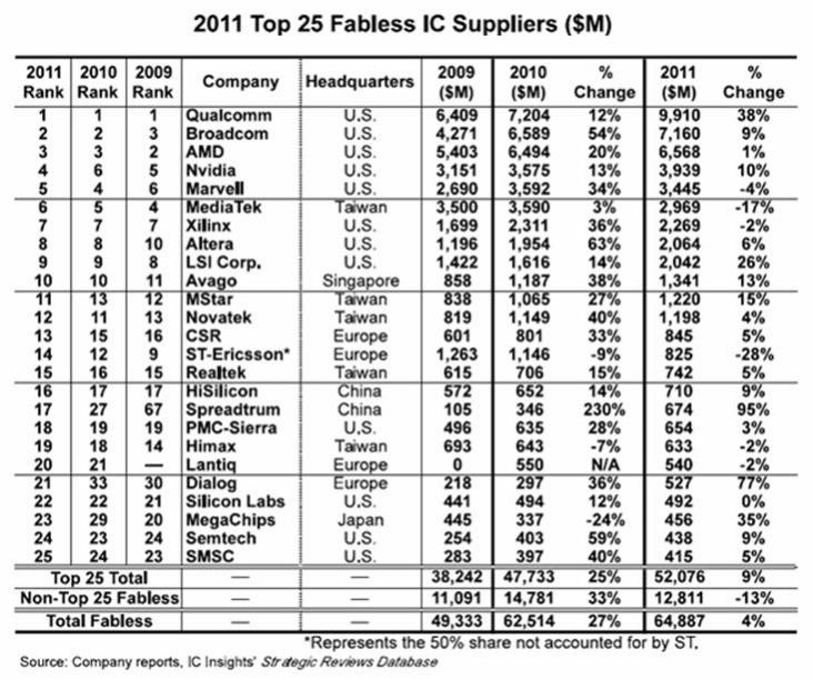
(Click to enlarge)
Fabless semiconductor companies were not forecasting growth, in fact, they were not forecasting at all since the forecasters that did not anticipate the recession were busy looking for jobs. Notice the +27% delta from 2009 to 2010. Not in the forecast, not even close.
Now lets look at the 28nm competitive landscape. The new iProducts, my iPhone 4s and my new iPad all contain 45nm Samsung Silicon. Not 28nm, not even 32nm but old school 45nm. And why is that Mr. Samsung? TSMC is the ONLYfab shipping 28nm silicon and there is definitely not enough to go around. Who plans on 100% penetration in any market segment? You can always hope for it but only a fool would bet money on it, and certainly not a modest company like TSMC.
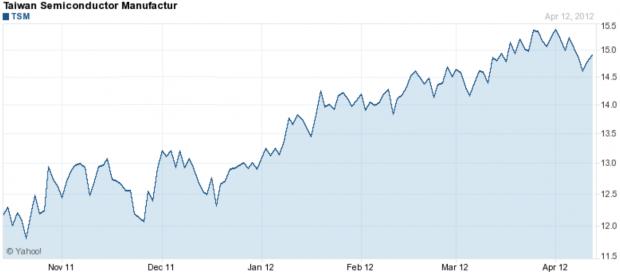
So there you have it, the semiconductor ramping process in a nut shell. If you would like to learn more about the semiconductor industry you can contact the Coleman Research Group and rent me for $300 per hour and I will explain everything to you in great detail wthout using acronyms. The Wall Street types do this on a regular basis and my bank account thanks you! TSMC stock (TSM) also thanks you as it is ramping quite well too.

20nm on the other hand may be a much more difficult ramp but it is too soon to say for sure. And do not expect to see 14nm production silicon until well into 2015, no matter what Samsung is telling you, just my opinion of course.
About TSMC
TSMC created the semiconductor Dedicated IC Foundry business model when it was founded in 1987. TSMC served about 470 customers and manufactured more than 8,900 products for various applications covering a variety of computer, communications and consumer electronics market segments. Total capacity of the manufacturing facilities managed by TSMC, including subsidiaries and joint ventures, reached above 9 million 12-inch equivalent wafers in 2015. TSMC operates three advanced 12-inch wafer GIGAFAB™ facilities (fab 12, 14 and 15), four eight-inch wafer fabs (fab 3, 5, 6, and 8), one six-inch wafer fab (fab 2) and two backend fabs (advanced backend fab 1 and 2). TSMC also manages two eight-inch fabs at wholly owned subsidiaries: WaferTech in the United States and TSMC China Company Limited, In addition, TSMC obtains 8-inch wafer capacity from other companies in which the Company has an equity interest.
TSMC’s 2015 total sales revenue reached a new high at US$26.61 billion. TSMC is headquartered in the Hsinchu Science Park, Taiwan, and has account management and engineering service offices in China, Europe, India, Japan, North America, and, South Korea.
Share this post via:


Comments
0 Replies to “The Truth of TSMC 28nm Yield!”
You must register or log in to view/post comments.