You are currently viewing SemiWiki as a guest which gives you limited access to the site. To view blog comments and experience other SemiWiki features you must be a registered member. Registration is fast, simple, and absolutely free so please,
join our community today!
WP_Term Object
(
    [term_id] => 158
    [name] => Foundries
    [slug] => semiconductor-manufacturers
    [term_group] => 0
    [term_taxonomy_id] => 158
    [taxonomy] => category
    [description] =>
    [parent] => 0
    [count] => 1350
    [filter] => raw
    [cat_ID] => 158
    [category_count] => 1350
    [category_description] =>
    [cat_name] => Foundries
    [category_nicename] => semiconductor-manufacturers
    [category_parent] => 0
    [is_post] =>
)
-Samsung said its not reducing its capex despite downturn
-A clear indication they want to take share/kill Micron & others
-Is the US government subsidizing predatory chip behavior?
-The last US memory chip maker is clearly threatened
Samsung announces worst results in 8 years
Samsung released its earnings which were the… Read More
-Samsung off the same chip cliff as Micron- “No skid marks”
-Samsung may be winning at a game of “Capex Chicken”
-No expectation of recovery any time soon – Consumers weak
-2023 a write off- Recovery will be delayed if spending isn’t
Samsungs worst quarter in 8 years no surprise
Samsung pre… Read More
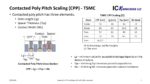
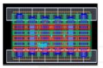
TSMC presented two papers on 3nm at the 2022 IEDM; “Critical Process features Enabling Aggressive Contacted Gate Pitch Scaling for 3nm CMOS Technology and Beyond” and “A 3nm CMOS FinFlexTM Platform Technology with Enhanced Power Efficiency and Performance for Mobile SOC and High Performance Computing Applications”.
When … Read More
The world of analog cell design and migration is quite different from digital, because the inputs and outputs to an analog cell often have a continuously variable voltage level over time, instead of just switching between 1 and 0. Kenny Hsieh of TSMC presented on the topic of analog cell migration at the recent North American OIP … Read More
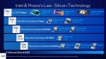
Ann Kelleher is Intel’s Executive Vice President, General Manager, Technology Development, and she gave the first plenary talk to kick off the 2022 IEDM, “Celebrating 75 Years of the Transistor A Look at the Evolution of Moore’s Law Innovation”. I am generally not a fan of plenary talks because I think they are often too broad and… Read More
Successful ASIC providers offer top-notch infrastructure and methodologies that can accommodate varied demands from a multitude of customers. Such ASIC providers also need access to best-in-class IP portfolio, advanced packaging and test capabilities, and heterogeneous chiplet integration capability among other things.… Read More
After attending the TSMC and Samsung foundry conferences I wanted to share some quick opinions about the foundry business. Nothing earth shattering but interesting just the same. Both conferences were well attended. If we are not back to the pre pandemic numbers we are very close to it.
TSMC and Samsung both acknowledged that there… Read More
On November 10th I watched the presentation by L.C. Lu, TSMC Fellow & VP, as he talked about enabling system innovation with dozens of slides in just 26 minutes. TSMC is the number one semiconductor foundry in the world, and their Open Innovation Platform (OIP) events are popular and well attended as the process technology and… Read More
This was the 12th TSMC OIP and it did not disappoint. The attendance was back to pre pandemic levels, there was interesting news and great presentations. We will cover the presentations in more depth after the virtual event which is on November 10th. You can register HERE.
As I mentioned in my previous post, the Jim Keller Keynote … Read More
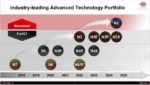
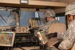
This will be the year of the semiconductor foundry ecosystem, absolutely. Right in between the Samsung SAFE Forum and the TSMC OIP Open Ecosystem Forum, Intel Foundry Services (IFS) just announced a United States Military, Aerospace, and Government (USMAG) Alliance.
Brilliant move, of course, due to the US Government now being… Read More


Agentic AI Demands More Than GPUs