The successful transition to a new fabrication process from development to high volume manufacturing requires a collective, collaborative effort among process engineers, equipment manufacturers, and especially, chemical suppliers. Of particular importance is the chemistry of the photoresist materials and their interaction with the exposing photons/electrons representing the pattern data for each mask layer.
The transition to high numerical aperture (“high NA”) lithography for future process nodes will entail not only tremendous engineering innovation from the system provider (e.g., ASML), but also advanced development of suitable photoresist materials.
At the recent VLSI 2021 Symposium, James Blackwell from Intel’s Components Research Group provided an extremely insightful look into the selection and optimization of potential photoresists for the upcoming high NA EUV transition.[1]
The clear take away from his talk is that finding a suitable photoresist is still a very active area of research, which must proceed concurrently with the system development (using a EUV source other than a full scanner system). This article summarizes the highlights of the presentation, specifically focusing on the challenges ahead to enable high NA EUV to achieve high volume manufacturing.
Background
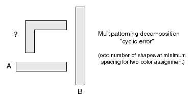
A watershed moment in our industry over the past decade was the introduction of multipatterning lithography, to enable continued scaling of design pitch on critical layers. To achieve a pitch less than ~80nm, with 193nm wavelength exposure with immersion (193i), it was necessary to divide the mask data into distinct subsets. Shapes were “colored” with a subset designation – e.g. “A” and “B” mask data for double patterning lithography. Process design kit layout rules were extended to reflect support for the algorithms used to subset the full layer data. Design rule verification functionality was extended to perform “cyclic” checking, to confirm that the data decomposition into resolvable shapes would be successful at the mask house. For example, a cyclic decomposition error is illustrated below.[2]
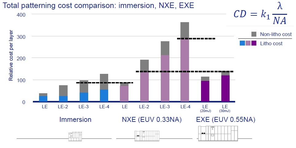
The full layer patterning was realized with a sequence of “litho-etch” steps for each mask subset – e.g., LE-2, LE-3, and LE-4 designates a process flow for double, triple, and quad patterning, respectively.
Additionally, the mask-to-mask overlay tolerance at each multipatterning layer introduced a new source of process variation. The distance between adjacent wires on the same metal layer, and thus their coupling capacitance, varies with the LE-LE process window.
The evolution of multipatterning also resulted in increased fabrication cost; the trend in “decreasing cost per transistor” guided by Moore’s Law abated. As alluded to above, with continued adoption of multipatterning in successive process nodes, LE-2 evolved to LE-3 and LE-4, further contributing to higher costs, as depicted below.[3]
EUV
Frequent SemiWiki readers are no doubt familiar with the recent evolution of extreme ultraviolet (EUV) lithography systems with a wavelength of 13.5nm, to displace 193i litho. To intercept the rising cost trends of multipatterning, EUV systems have achieved production status, in terms of exposure throughput (wafers per hour), exposure intensity, and system uptime. As depicted in the figure above, active R&D work is underway to release a 2nd generation EUV system. This system will incorporate a higher numeric aperture (NA = 0.55) in the lensing path, enabling finer pitch resolution, and again recalibrating the cost per layer trend from EUV multipatterning with first generation NA=0.33 equipment.
EUV systems are a marvel of engineering, to be sure. Yet, an often underappreciated facet of the EUV litho evolution is the corresponding development efforts for a corresponding photoresist material.
Photoresist Basics
Briefly, selective exposure of a photoresist-coated wafer to high-energy photons (or high-energy electrons) results in a change in the chemical bonding configuration of the original material. For a (positive) organic photoresist polymer, the incident photon results in a “deprotection” chemical reaction; a subsequent step immerses the exposed wafer into a developer, which dissolves the deprotected polymer. While the dimensional targets are tighter with each new process node, the fundamental goals haven’t really changed:
- high absorbance and selectivity to the photon wavelength/energy (E=h*f)
- goal is a lower photon dose (mJ/cm**2), and greater exposure latitude
- high contrast
- low scattering of the chemical reaction
- high developer selectivity to chemical configuration differences
- goal is to reduce the “line edge roughness” (LER) of the developed image
- low viscosity
- ease of photoresist application; a thin, uniform PR layer (after spin-coat and pre-bake) is needed, as the depth-of-focus for EUV exposure is very small
- good adherence to the wafer substrate surface
- ease of photoresist removal, after the etch step
For recent process nodes, chemically-amplified resist (CAR) materials have been introduced. The CAR composition introduces a “photoacid generator” (PAG) to the resist. In simplest terms, a photoacid is a molecule which releases protons (H+) upon light absorption, called photodissociation. After exposure, a subsequent heating step releases the acid, which acts as a catalyst to the polymer fragmentation.
The acid is not consumed in the deprotection, and continues to diffuse through the resist to provide (hundreds of) reactions, thus amplifying the impact of the photon energy dose. An inhibitor (or “quencher”) compound is also incorporated into the CAR, attached to the resist polymer chain. This acid-soluble inhibitor mitigates the acid diffusion and improves the dissolution contrast, reducing the resulting LER.
The thin photoresist film thickness associated with the low depth-of-focus for EUV litho, combined with the goal of a reduced dose for improved system throughput/uptime, implies that EUV exposure is a stochastic process, with (random) variation in the incident photons/unit area density.
Non-uniformities in density of the polymer-CAG-inhibitor components are another source of variation. Another difficult tradeoff with the transition to thin organic photoresist films is the need to be sufficiently robust to the post-patterning etch (or implant) process step. Thicker PR layers would be more robust to the subsequent step, but would be more difficult to resolve at lower exposure dose. A high aspect ratio developed PR film is subject to “pattern collapse”, as illustrated below. [4]

The surface tension of the developer solution would collapse the spacing between adjacent, tall PR lines.
As a result, process engineers are focused on improved EUV metrology to uncover lithography defect mechanisms – e.g., incompletely developed lines and vias. Another indication of the strong interdependencies in the EUV evolution is the semiconductor equipment provider focus on fast, in-line lithography inspection.
Resists for High NA EUV
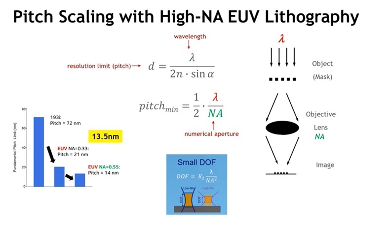
The data James presented were the result of a close collaboration between Intel, photoresist suppliers, academic institutions, and research labs. The figure below illustrates the targeted transition in photolithographic pitch enabled by high NA EUV, and the requirement for thinner resist coating for the reduced depth-of-focus.
Prior to the availability of high NA EUV systems, how does a materials engineer evaluate potential photoresist materials? James described a system that Intel developed specifically for photoresist research, as illustrated below.
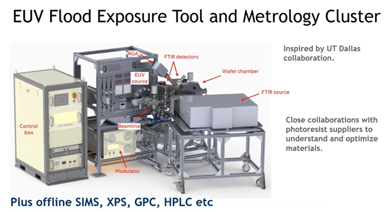
A EUV source is connected to a wafer chamber. James highlighted the Fourier Transform Infrared Spectroscopy (FTIR) detection features added to the system. (FTIR uses the absorption of a material across an infrared spectrum exposure to provide an analysis of a material; it can provide real-time data on the concentration of reactants and products of a chemical reaction.) This system has enabled Intel to gain insights into the photoresist response to EUV exposure.
A unique facet of EUV photoresist R&D is the potential to use metal-oxide resist chemistry, as an alternative to the traditional polymer materials. These “inorganic” resists have high EUV absorptivity, and high etch resistance for subsequent processing. The figure below provides a simplified comparison of the metal-oxide versus organic resist chemistry.[5]
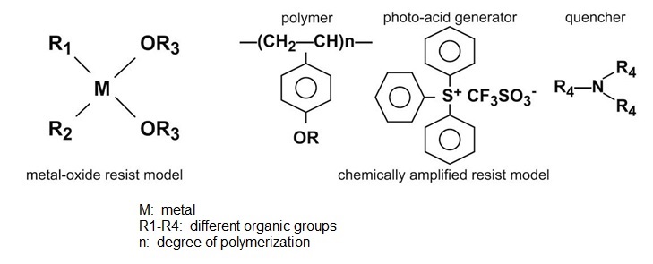
James described one option for a metal-oxide resist, utilizing Hf-O-C. (Oxides of Ti and Zr are also actively being investigated in the industry.) The chemical reaction sequence for the resist is depicted below – the FTIR analysis confirmed the presence of CO2 during the reaction, and the cross-linking of Hf-O-C clusters as the result.
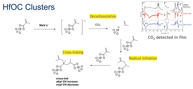
Note the cross-linking after exposure differs from photodissociation described earlier, where the solubility “switch” is now associated with a negative resist.
James also described results with organic CAR resists for EUV exposure. An example of proposed resist (plus PAG plus inhibitor) chemistry, and a corresponding contrast versus dose curve are shown below.
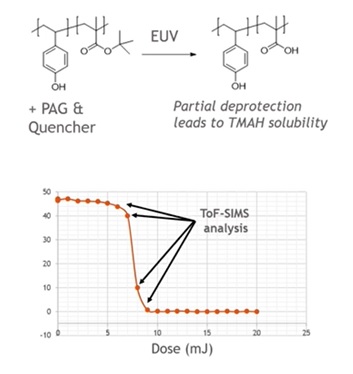
As mentioned earlier, non-uniformity of the resist composition contributes to increased variation in the developed image. James described an experiment the Intel team had pursued to evaluate the homogeneity of the resist, as illustrated below.

In this case, secondary ion mass spectroscopy (SIMS) was used to analyze the thin film composition over a focused incident ion beam size, and aggregating a large number of samples to assess the PR heterogeneity.
In James’ words, “This SIMS method provided data to guide us to chemical changes that led to improved patterning uniformity. Better analytical methods are required to improve EUV resist design for the challenges introduced by high NA EUV – such as SIMS and FTIR for metal-oxide resists. And, close collaboration with suppliers is critical.”
Summary
The introduction of high NA EUV systems will be a key step in addressing the cost concerns associated with EUV multipatterning. Yet, as this Intel presentation at the VLSI Symposium 2021 illustrates, there clearly remains a considerable amount of development (and qualification) ahead to meet the corresponding photoresist materials requirements, especially addressing the tradeoffs between organic versus metal-oxide materials. It will be very interesting to see how the concurrent and strongly interdependent lithographic system and photoresist technologies evolve.
-chipguy
References
[1] J. Blackwell, “Mechanism and Materials for Advanced Patterning”, VLSI Symposium 2021, Workshop 4.
[2] Dillinger, T., VLSI Design Methodology Development, Prentice-Hall.
[3] van Schoot, Jan, et al., “High-NA EUV Lithography Exposure Tool for EUV Roadmap Extension”, EUV-FEL Workshop, January 22, 2021.
[4] Luo, C., et al., “Review of recent advances in inorganic photoresists”, Royal Society of Chemistry Journal, Vol. 10, 8385-8395.
[5] De Simone, D., et al., “Novel metal-oxide photoresist materials for extreme UV lithography”, SPIE News, July 1, 2016.
Share this post via:


Comments
4 Replies to “Resist Development for High-NA EUV”
You must register or log in to view/post comments.