At the recent ISSCC conference, Mozhgan Mansuri from Intel gave an enlightening (extended) short course presentation on all thing related to clocking, for both wireline and wireless interface design. [1] The presentation was extremely thorough, ranging from a review of basic clocking principles to unique circuit design strategies for synthesizing and distributing clocked signals.
Personally, I found her talk to be both an excellent refresher and a source of lots of new information (for me, at least) – I thought the highlights of her talk might be of interest to SemiWiki readers. There was a plethora of topics covered – I’ll focus on the wireline-based design considerations. I would encourage you to review her ISSCC short course material, both wireline and wireless clocking features.
Wireline DataRate Trends
A graph depicting the progress in wireline “per lane datarates” is shown below, for several interface standards.
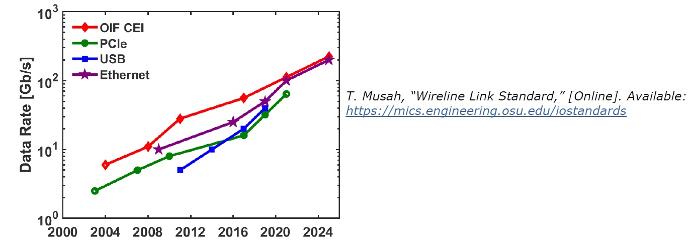
The PPA benefits of Moore’s Law is paralleled by interface datarate enhancements, doubling every ~2-3 years. Yet, as wirelines span silicon, packaging, board interconnect, connectors, and cables, silicon technology scaling alone does not account for all of the datarate enhancements. Improvements in package/PCB materials and simulation tool advances have certainly helped.
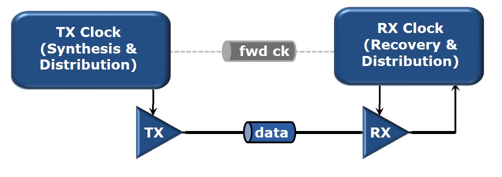
The key to this growth has been the ongoing interface circuit enhancements supporting the Tx and Rx ends of the lane. The associated clock generation (and Rx clock recovery) techniques have been at the heart of those circuit innovations as depicted below, showing both embedded clock in data and forwarded clock options.
Clock Definitions
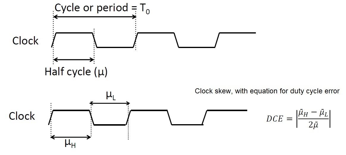
The basic clock definitions are shown below:
- clock period
- (50/50) duty cycle
- clock skew (static duty cycle error, the difference between the half cycle durations)
- jitter between cycles (dynamic; both deterministic (e.g., due to supply voltage variations) and random (e.g., due to thermal and flicker noise in devices))
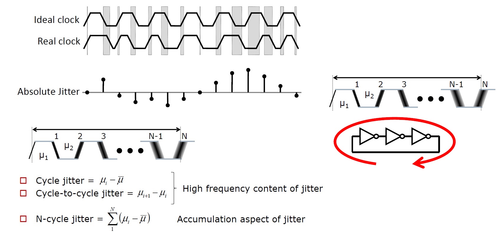
Note in the last figure above that jitter may accumulate over time, as depicted for the odd-inverter, free-running oscillator clock source.
The figure below illustrates two key measurements (and specs) for clock distribution. The first half of the figure illustrates the frequency response of a circuit to the jitter frequency content; the second illustrates the “tolerance” of the Rx clock recovery circuitry to jitter.
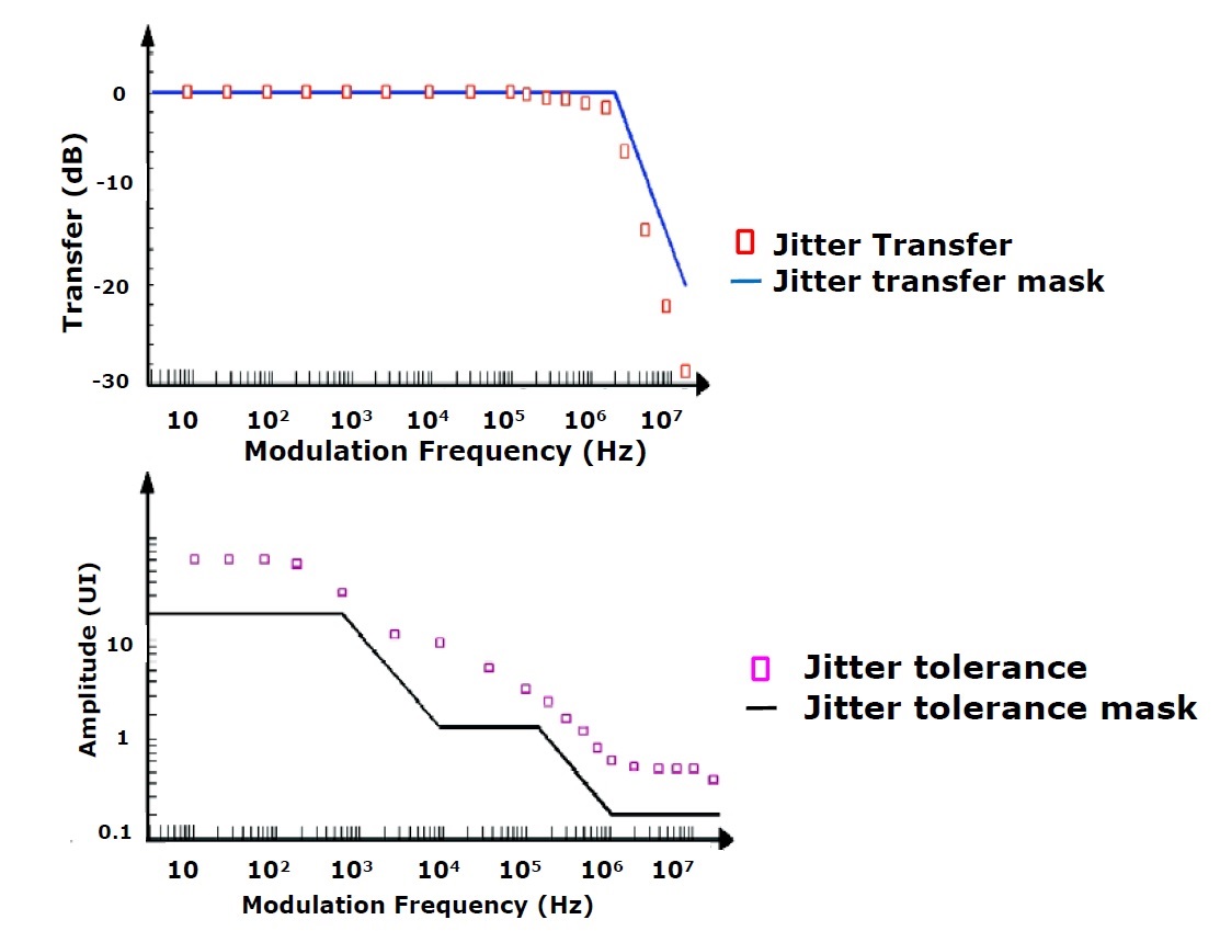
The figures include a typical specification “mask” over frequency. The “ideal” jitter transfer curve depicted above provides a “0 dB, no jitter amplification” target mask through a clock distribution component. The jitter tolerance mask spec enables designers to develop the Rx clock recovery circuitry, subsequently ensuring that the Tx jitter sources do not exceed the mask limits.
Clock Synthesis Circuitry
To generate high-frequency clocks on-chip, the common method is to employ one of two main circuit types – a phase-locked loop (PLL), and a delay-locked loop (DLL). Their principal function is to provide a “multiplied” clock output derived from a lower-frequency (high-quality) reference clock, as described below. Another key clock synthesis configuration is used to phase-align individual clocks tapped from an on-die oscillator, with an “injection locked oscillator” (ILO).
- PLL

The PLL consists of:
- a voltage-controlled oscillator – e.g., a free-running oscillator with adaptive response to an input voltage signal that modulates the oscillator loop delay (examples given shortly)
- a divide-by-N counter (the multiplicative factor of the PLL)
- a phase detector, that provides an output signal proportional to the leading/lagging phase difference between the reference and divided VCO clocks (example shortly)
- a low-pass filter that effectively blocks short-duration signals from the phase detector from influencing the control input to the VCO
The frequency bandwidth response of the PLL defines the jitter response, a key design tradeoff. For example, a lower bandwidth will reduce the sensitivity to jitter in the reference clock input. A higher bandwidth will reduce the sensitivity to VCO jitter.
- DLL

The figure above illustrates the principles underlying a (multiplying) delay-locked loop (DLL). The free-running VCO oscillator in the PLL is replaced by a delay line, whose individual delay elements are controlled by the phase-detector and low-pass filter output – in the figure, a simple inverter delay chain is shown. The jitter in the DLL clock output is “reset” by using the reference clock edge every N cycles, using the multiplexer output providing the delay chain input – see the timing diagram in the figure.
- Injection Locked Oscillator
Another option for clock synthesis is the use of injection current into an oscillating system to provide output clock phase adjust control.
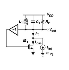
A high-level block diagram of the ILO is shown below. [2] There are three components of note:
- an oscillator (depicted simply as an nFET and inverting amplifier)
- a tuned tank circuit
- the injection current source
Recall the physics experiment where multiple metronomes of (nominally) the same time period are loosely-coupled – over time, they will synchronize (YouTube video link).
An injection current of frequency f will similarly synchronize the output voltage of the combined system to this frequency. However, due to the relative impedances of the three components, there will be a resulting phase shift between the system output voltage and the constituent currents I_tank, I_osc, and I_inj, as depicted below.
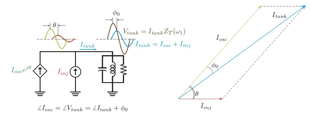
In short, Vout = (Z_tank * I_tank), where I_tank = (I_osc + I_inj). These are complex quantities with both magnitude and phase. The key feature of the ILO is that the magnitude of the injected current adjusts the phase of the output voltage.
The ILO is thus an ideal method to align (or “rotate”) the phase of a clock output, relative to a reference – the phase difference detector increases/decreases the magnitude of the injected current accordingly.
Consider the case where it is desirable to generate clocks from multiple internal stages of an oscillator, each clock shifted/aligned by a specific phase. The example below shows 4 clocks of the same frequency, each phase shifted by 90 degrees.
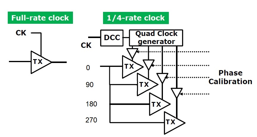
Logical operations on these shifted clocks derive unique pulses – e.g., clock_0 AND clock_270. When presented with data training patterns with transitions corresponding to logical operations of these shifted clocks, phase differences between the data and clock pulses can be detected and aligned using the injection lock current. Once aligned, the clocks can then be used to transmit/receive data at a high datarate – 4X the reference clock frequency, in the example above.
The previous discussion referred to the block diagrams of the clock generation circuitry – Mozhgan elaborated on these units in her presentation.
- VCO
Examples of a voltage-controlled oscillator from her talk is shown in the figure below.
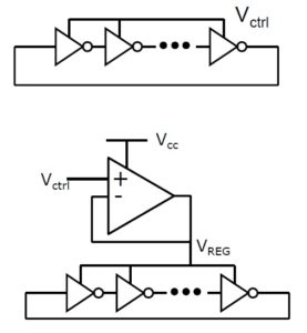
The first example is a simple (odd-numbered) loop of inverters, providing a free-running oscillation – the delay of each stage is modified by the voltage control signal. (Other means of introducing delay control are also frequently used – e.g., adding a variable capacitive load to each stage using a varactor; using “current-starved” inverters with an additional series nFET/p/FET in the pulldown/pullup stack, whose device gates provide voltage control input.) A disadvantage of this free-running topology is the sensitivity to noise on the supply/control input.
The second example shown above includes an operational amplifier/regulator as a low-pass filter to improve the supply noise rejection.
- Phase Difference Detector
The clock generation circuits that compare a reference to a (divided) clock use a phase difference detector to provide the control signal(s) to the VCO. There are numerous detector topologies in common use – a simple (digital) example implementation is shown below. [3, 4]
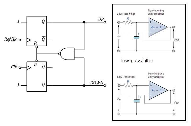
This topology fits with the oscillator control circuits that use two inputs – “UP” and “DOWN” to represent a lagging/leading phase difference between the reference and generated clock. (A low-pass filter is needed to remove any spurious flop output pulses between the rising clock and asynchronous reset input.)
Clock Distribution
Mozhgan presented some of the common design topologies for distributing an on-die generated clock to the (Tx or Rx) fanout. The figure below depicts three examples, for the case where a single (global) clock spans a considerable distance before being tapped to a series of sinks:
- a (differential, low-swing signaling) repeaterless topology, regarding the interconnect as an LC transmission line
- an inverter repowering chain
- a chain driven by (differential) current-mode logic inverters
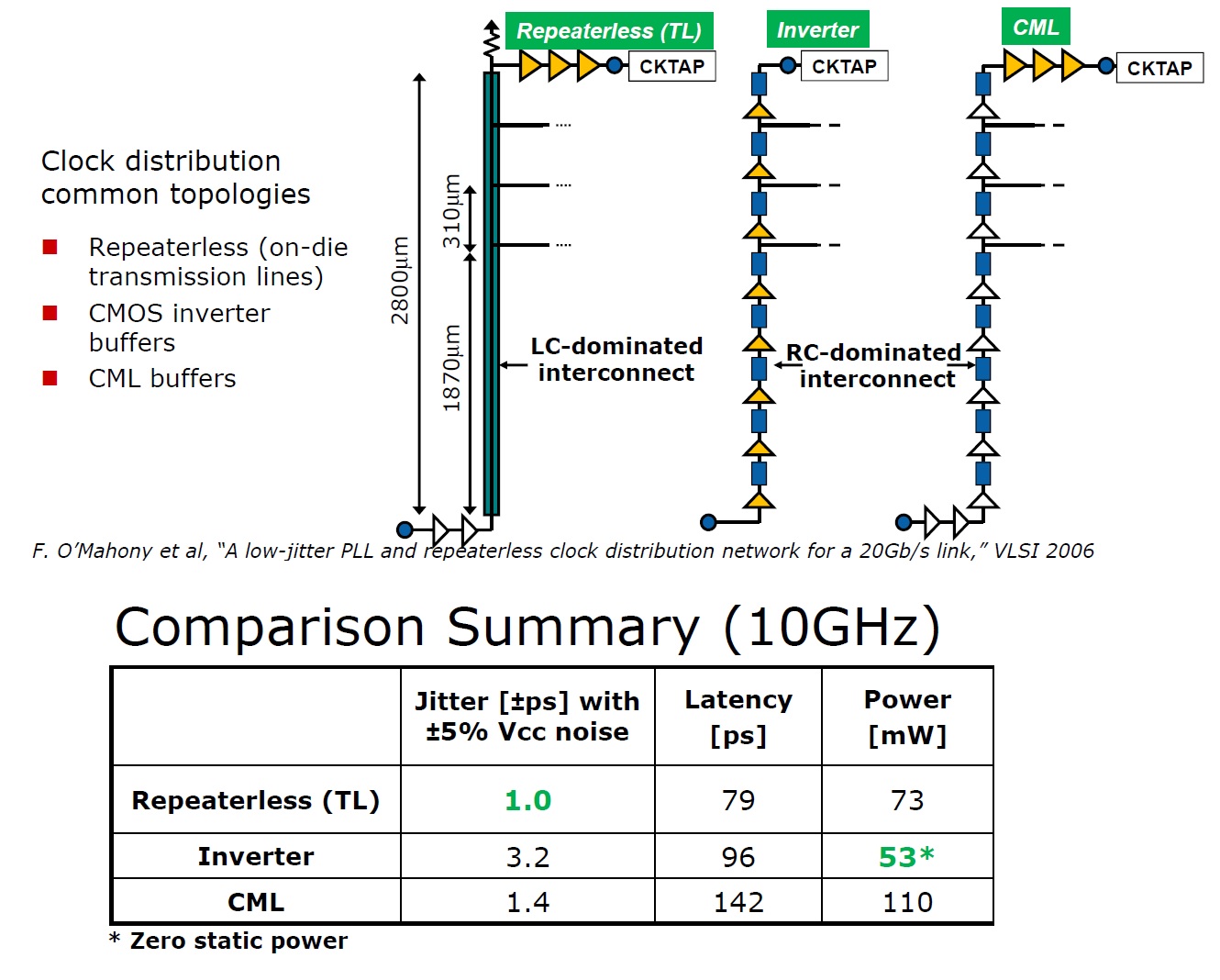
(The differential methods require additional circuitry at the clock sinks.) These topologies present different tradeoffs, relative to: jitter, phase skew, impact on slew rate from bandwidth losses, power dissipation, and power supply noise rejection. Clock distribution planning is clearly an integral part of developing a Tx or Rx interface solution.
Mozhgan’s presentation covered a wealth of additional topics, not highlighted here – e.g., wireline Rx clock-data alignment strategies (for both forwarded clock and embedded SerDes clock interfaces), clock generation for wireless transmission/receivers, clock power optimization. Hopefully, the few topics presented here have whetted your appetite to learn more about the unique characteristics of Tx/Rx clocking. I would encourage you to review Mozhgan’s ISSCC presentation.
-chipguy
References
[1] Mozhgan Mansuri, “Clocking, clock distribution, and clock management in wireline and wireless subsystems”, ISSCC 2021, Short Course SC-3.
[2] http://rfic.eecs.berkeley.edu/ee242/pdf/Module_7_4_IL.pdf
[3] https://analog.intgckts.com/phase-locked-loop/phase-frequency-detector/
[4] https://www.electronics-tutorials.ws/filter/filter_5.html
Share this post via:


Comments
There are no comments yet.
You must register or log in to view/post comments.