Bob Swan started as interim CEO in June of 2018 and took the full-time CEO job in January of 2019. I was a vocal critic of the previous CEO Brian Krzanich (BK) and really felt he was not fit to serve. As it turns out I was right. It is not just the CEO himself, but also the people that he surrounds himself with. BK surrounded himself with the Intel old guard and a couple of questionable newcomers, the rest is history.
I do have to thank BK as he is one of the reasons why I am somewhat famous or infamous. We had a very public feud back in the dark days of Intel 14nm and 10nm.
While I am not a fan of CFOs (followers) who become CEOs (leaders) I have high hopes for Bob Swan and the people with whom he will surround himself.
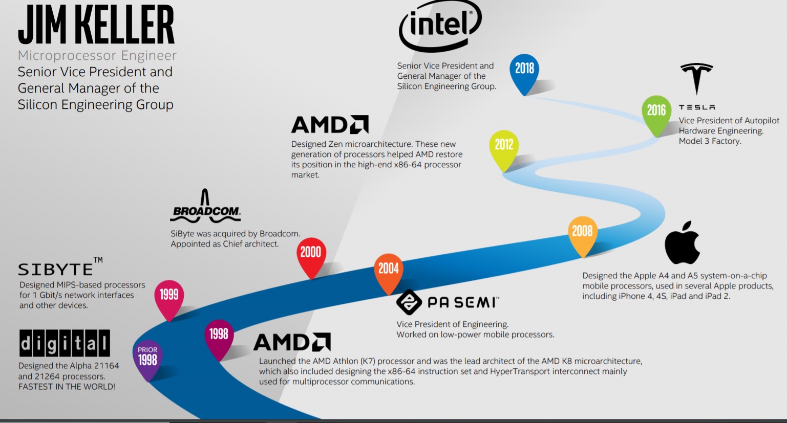
If you take a look at the Intel executive staff today there have been quite a few changes, most notably the addition of Jim Keller as senior vice president in the Technology, Systems Architecture and Client Group (TSCG) and general manager of the Silicon Engineering Group (SEG). Jim is responsible for “architecting the silicon engineering organization within TSCG”. This is a seriously disruptive move on the part of Intel.
For those of you who have not heard of Jim here is his career path graphic:

Jim is mentioned in our book “Mobile Unleashed” in the Apple chapter by the way. PA SEMI figured prominently in the success of the Apple SoC efforts. Jim really is a Silicon Valley legend amongst us semiconductor soldiers in the SoC trenches.
To get a better understanding of Jim Keller take a look at his recent Youtube video he did entitled Jim Keller: Moore’s Law is Not Dead:
It is a full hour but well worth your time, especially if you are one of the ill-informed who think Moore’s Law is dead.
Back to Bob Swan and 10nm, 7nm, 5nm, and 3nm. In the recent conference call Bob mentioned that Intel will get back to the Tick-Tock two year cadence where Tick is a new process and Tock is a new product architecture. Here are some cut/pasted comments from Bob:
The Intel 10-nanometer product era has begun and our new 10th Gen Core Ice Lake processors are leading the way. In Q3, we also shipped our first 10-nanometer Agilex FPGAs. And in 2020, we’ll continue to expand our 10-nanometer portfolio with exciting new products including an AI Inference Accelerator, 5G base station SoC, Xeon CPUs for server storage and network and a discrete GPU. This quarter we’ve achieved power on exit for our first discrete GPU DG1 an important milestone.
We are on track to launch our first 7-nanometer based products, a data center focused discrete GPU in 2021 two years after the launch of 10-nanometer. We are also well down the engineering path on 5-nanometer.
Back in our Analyst Day, we tried to go through this in quite a bit of detail, both, one, kind of our lessons learned coming out of the challenges we had with 10 and how we’re capturing those lessons learned as we think about the next two generations. But first our focus and energy is right now around scaling 10.
And, as we said, we feel very good about the capacity we put in place, the products we have coming down the pipeline and the yields that we’re achieving, almost week-on-week improvement over the last six months. So for 10, we feel really good.
Second, when we put the design rules in for 7-nanometer, we were less aggressive in terms of density. Our learning from going from 14 to 10 is with a benefit of hindsight, we were just — we tried to scale at a 2.7 factor and that was — that ended up putting too much invention or revolutionary nodes into the fab environment to meet those kind of hurdles and the learning from that is, we just can’t hit those kind of really aggressive targets, when, to your point, the dynamics are getting increasingly challenging. So lots of learnings out of 10. Our transition to 10 that we incorporated into 7, the design the design rules there’s less complexity and for the last couple of years that we’ve been working with EUV.
Litho has been the challenge. We’ve had EUV that we’ve been working with for a few years now and we expect to use EUV as we scale 7. And we indicated that our first product will be two years from this quarter. So fourth quarter of 2021, our first 7-nanometer product will come out and our expectation is that we’ll get back on a two-year cadence from 7 and beyond. So lots of learning out of 10-nanometer that we’ve incorporated, and we said back in May and we reiterated today, we expect to be back to a two to two-and-a-half year cadence going forward at least for the next few nodes.
Bottom Line: Intel got too aggressive at 10nm with 2.7x scaling without EUV and the design rules were much too complex for the process maturity. Intel 10nm is finally in HVM after a four year delay and 7nm is well under way. EUV is in HVM at TSMC, TSMC did the heavy EUV lifting, so I have confidence Intel will get 7nm in 2H 2021, hopefully.
Intel 7nm will be FinFETs (yawn) but Intel 5nm will be horizontal nanosheets and Intel 3nm CFETs. Interesting times ahead at Intel, absolutely!
Share this post via:


Comments
5 Replies to “Intel CEO Update Q4 2019”
You must register or log in to view/post comments.