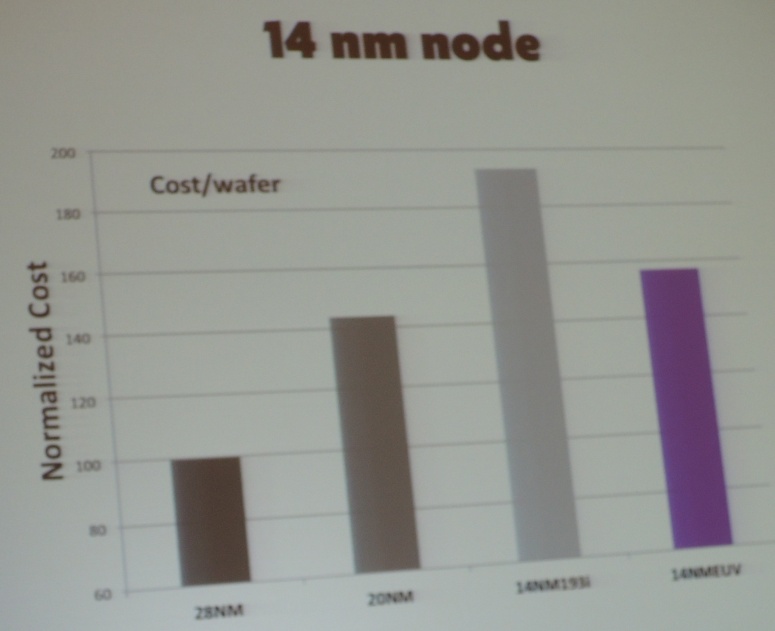
I didn’t attend the International Electronic Device Meeting (IEDM) earlier this month, but there have been a lot of reports on the inter webs especially about 20nm and 14nm processes. Some of this is really geeky stuff but I think that perhaps the most interesting thing I’ve read about is summarized in this chart:

This shows the wafer costs (12″, 30cm wafers) for 28nm, 20nm and then 14nm with multiple patterning and, in purple, 14nm with EUV lithography. The chart comes from Luc van den Hove, chief executive of IMEC in Belgium.
These are raw wafer costs and thus haven’t been adjusted for the increase in transistor (and perhaps interconnect) density. Typically when we transition from one process node to the next, the wafer costs go up a little bit but that is completely dominated by the increase in how much we can put on a given sized die, and so the cost per transistor drops substantially. This is the economic driver of Moore’s law and is what makes it possible to have a $500 iPhone deliver more computer power than a 1980s mainframe that cost millions of dollars.
But these costs are going up dramatically. The Y-axis scale doesn’t start at zero so the picture is a bit misleading, 14nm costs are not three times 28nm. But they are nearly twice. If the process truly scaled everything then the density of transistors at 14nm would be four times that of 28nm so cost per transistor would still be falling fast. But increasingly the transistor length is only the headline number for the process and the interconnect is shrinking much more slowly, if at all. When you look at the pitches for various layers in a modern process it is impossible to see anything close to 2X the headline number.
So the key question is whether 14nm will have an economic driver or just a technology driver for those few designs that can truly take advantage of the increased density and decreased power, even though there may even be a cost penalty. For Apple’s iPhone and Samsung’s Android phones probably. For those $50 smartphones for developing countries that won’t work.
Despite the purple bar looking optimistic, the received wisdom is that EUV is now too late for 14nm and so we will have to have a lot of double and triple patterning instead (which is one of the things that drives the cost up so much). EUV works in the sense that you can flash some wafers but the current state-of-the-art seems to be about 20 wafers/hour versus the 100 or 200/hour that is required to make the approach viable. The intensity of the light source (droplets of tin zapped with a huge laser) is too low, the mirrors (which aren’t really mirrors in the usual sense) absorb too much of the light, and there are too many reflections required between the source and the photoresist. Not much energy makes it to the resist to make the exposure.
On a more optimistic note, Intel claimed that their costs per transistor were falling with each process node. Apparently they also don’t use double patterning at 20nm and there are two reasons for this. Firstly, they can have as restrictive design rules as they like, since they are the ultimate IDM with a limited product range. Secondly, most of the pitches at 20nm are not much different from 28nm. As I said above, only the FinFET transistor is 20nm or 22nm long.
Anyway, 2013 will be the year we find out what 20nm and 14nm really can deliver as these processes start to ramp up. As Yogi Berra said, “the future ain’t what it used to be.” (although you have to be careful with Yogi Berra quotes. As he also (maybe) said, “I didn’t say all the things I said.”)


Comments
0 Replies to “Wafer Costs: Out of Control or Not?”
You must register or log in to view/post comments.