Introduction
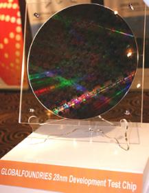
Monday morning at DAC I attended the breakfast presentation from Magma, ARM and GLOBALFOUNDRIES. The 28nm node is ready for business using Magma tools and ARM libraries.
During breakfast I met Karim Arabi, Ph.D. from QualComm. He’s a senior director of engineering in San Diego and wanted to learn more about the 28nm node and how Magma tools could be used in a flow.
Notes
Rod Metcalf – Magma, 28nm Reference Flow Development, using the Talus flow manager for the entire IC design flow. We ran a testcase to ensure silicon validation. Goal is to use the Magma flow on a 28nm Global Foundries process and get 1st silicon success.
– Use the existing libraries which are characterized at specific corners, or create your own corners.
– They used an OpenCore design as their reference example.
– ARM supplied the 28nm libraries, standard cells, memories. Multi Vt libraries were used.
– Talus from Magma: The RTL-to-GDS II tool flow. Offers high capacity, silicon proven at 28nm, high speed designs.
– Low power technologies used, CPF and UPF.
– Talus Flow Manager: a way to capture a complete tool flow. Analysis results are in HTML, easy to read or email complete with links for more details. Pie charts, timing violations.
– Talus Flow Manager – the reference flow provides correct setups for all tools needed, much less work for users to
GLOBALFOUNDRIES – Our largest competitor reports their test chips as tape-outs, we don’t count those as tape-outs.
Summary: Flow of Magma tools and ARM libraries on the GLOBALFOUNDRIES 28nm process are ready to go now, proven, validated.
Jim Ballingall, Ph.D. VP Marketing – GLOBALFOUNDRIES uses high K metal Gate (HKMG). Photo of a quad-core CPU with a GPU from AMD producing 500Gflops performance (beats Sandy Bridge from Intel).
– Ramp of HKMG process is going well. Gate first HKMG approach (Intel uses Gate last HKMG). Intel is using FUD, don’t believe it.
– Market requirements for foundry customers.
o 28nm SLP (Super low power) – low mask count, no stress engineering for lowest costs
o 28nm HPP (High performance process) – uses stressors, >3GHz performance,
– Gate first can be 10 to 20% smaller std cells with Gate First compared to Gate Last approach
– CPU speed versus cost: SLP is lower clock speed and lower cost, while HPP is higher speed and higher cost
Global Solutions – an ecosystem with EDA tool vendors, mask making, assembly. A successful program.
– Design Kits for 28nm SLP are ready now, HPP coming soon.
– Investment of $5.4B in 2011 for GLOBALFOUNDRIES.
Common Platform Partners – IBM, Samsung, ST (Fab synch agreement)
Dresden Fab 1 – plan for 1 million wafers per year at 45nm and below nodes
Fab 8 in NY – shell is complete, equipment moving in, on schedule. 60K wafers/month.
Multi Program Wafers (MPW) – run every quarter, fully subscribed, allow lower costs.
20nm – In development now, partnered with IBM. Results due in 2012/2013. First shuttles started in 2011 Q4.
Q&A
Q: What about fin FET?
A: Looks like a 14nm technology to us.
Q: Is 20nm Gate Last?
A: Yes, that’s true. We choose that for fewer design rules. Gate First was good down to 28nm. At 20nm litho dominates and we choose Gate Last.
Q: What about DFT?
A: We partner with companies like SynTest for DFT tools, they can be integrated into our Talus Flow Manager like any Magma tool.
Largest DAC Banner
Yes, it’s the number 1 EDA company, Synopsys:


Captain America: Can Elon Musk Save America’s Chip Manufacturing Industry?