


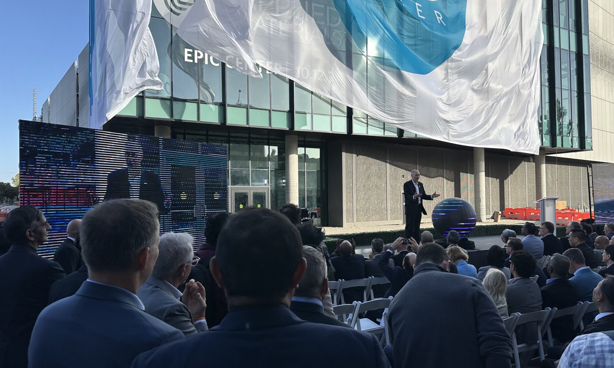


The semiconductor industry has long depended on collaboration between technology developers, equipment suppliers and manufacturers. But as artificial intelligence reshapes computing, established ways of working together may no longer be sufficient. The next wave of innovation will depend not just on what companies develop, but on how early they work together, how they share expertise and how quickly they can solve problems across organizational boundaries.
That was a central message in Applied Materials President and CEO Gary Dickerson’s keynote at the unveiling of the company’s EPIC Center. His perspective was that AI’s growing demands call for a different approach to research and development. An approach that brings partners together earlier and enables innovation across the entire semiconductor technology stack.
Move collaboration upstream
Traditional technology development can resemble a sequence of handoffs. One company develops a component or process, another works to integrate it, and further challenges emerge as the technology moves toward manufacturing and system deployment.
That approach becomes increasingly difficult when the performance of the final system depends on multiple technologies advancing together. Decisions about materials, equipment, transistor structures, interconnects, packaging, memory and system architecture can affect one another. Waiting until later development stages to address those dependencies can lead to costly redesigns and extended timelines.
A more effective model brings the relevant expertise into the process earlier. Rather than optimizing individual technologies against assumptions about what other parts of the system will deliver, partners can identify requirements and constraints together.
This creates opportunities to test ideas earlier, evaluate trade-offs jointly and pursue solutions that may be difficult for any company to develop independently. It also allows R&D teams to work in parallel on interdependent challenges instead of waiting for one stage to finish before another can begin.
Innovate across the technology stack
Dickerson’s vision extends beyond closer collaboration on individual projects. It calls for a broader view of semiconductor innovation, in which technologies are developed with the needs of the complete computing system in mind.
For AI infrastructure, that means connecting research in materials and manufacturing processes with advances in transistors, interconnects, memory integration and advanced packaging. Progress in one area must translate into meaningful improvements at the system level, including performance, energy efficiency and manufacturability.
This shift also changes how companies think about R&D priorities. The most valuable opportunities may lie at the boundaries between technologies, where a challenge cannot be resolved through improvements to a single component. Bringing different disciplines and organizations into the same development process can help uncover those opportunities earlier.
Trust is an operating requirement
Earlier collaboration creates another requirement: companies must be able to work together in a trusted environment.
Semiconductor companies operate in a highly competitive industry, and sensitive technical information cannot be shared without appropriate safeguards. Yet effective co-innovation often depends on partners understanding one another’s constraints, exchanging relevant expertise and addressing integration problems before they become expensive obstacles.
Trust is therefore more than a cultural aspiration. It is an enabler of technical progress. Companies need a shared understanding of what can be discussed, how information is protected and where joint work can create value. Establishing those conditions makes it easier for teams to engage earlier and tackle complex problems together.
The objective is not to remove competitive boundaries. It is to create the conditions in which companies can collaborate on shared technical challenges while protecting their individual interests.
EPIC as a model for co-innovation
The EPIC Center provides a physical setting for this approach. By bringing Applied Materials and industry partners together to work on next-generation materials, processes and equipment, it is intended to support more direct interaction and earlier experimentation.
Its larger significance is the model it represents: connecting expertise, aligning research priorities and tackling interdependent technology challenges before they become downstream integration problems. The value of such a model will ultimately be measured by what it enables: faster learning, more effective development and technologies that reach manufacturing and the market sooner.
As AI continues to expand the demands on computing, the semiconductor industry will need to innovate at a pace that individual organizations cannot always achieve working independently. Companies that can combine deep technical expertise with earlier engagement, parallel development and trusted collaboration will be better positioned to turn ambitious research into practical advances.
The next competitive advantage may depend as much on how the industry innovates as on the technologies it invents. EPIC reflects an effort to put that principle into practice.
For the industry-level explanation of why this change is needed, see the companion article, “The Industry Challenge: AI Is Forcing Semiconductor Innovation Beyond the Chip.”
Read the press release about the October 12th unveiling of the EPIC Center.
Also Read:
The Industry Challenge: AI Is Forcing Semiconductor Innovation Beyond the Chip
CEO Interview with Dr. Raj Talluri of Kulicke & Soffa
Podcast EP374: How proteanTecs Tames Multi-Die Packaging Challenges with Nir Server
Share this post via:


SEMICON West’s Autonomous Fab Vision Needs a Decision-Escalation Design