The world of analog cell design and migration is quite different from digital, because the inputs and outputs to an analog cell often have a continuously variable voltage level over time, instead of just switching between 1 and 0. Kenny Hsieh of TSMC presented on the topic of analog cell migration at the recent North American OIP event, and I watched his presentation to learn more about their approach to these challenges.
Analog Cell Challenges
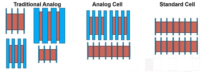
Moving from N7 to N5 to N3 the number of analog design rules have dramatically increased, along with more layout effects to take into account. Analog cell heights tend to be irregular, so there’s no abutment like with standard cells. Nearby transistor layout impacts adjacent transistor performance, requiring more time spent in validation.
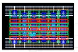
The TSMC approach for analog cells starting at the N5 node is to use layout with fixed cell heights, support abutment of cells to form arrays, re-use pre-drawn layouts of Metal 0 and below, and that are silicon validated. Inside the PDK for analog cells are active cells, plus all the other parameters for: CMOS, guard ring, CMOS tap, decap and varactor.
Analog cells now use fixed heights, placed in tracks, where you can use abutment, and even customize the transition, tap and guardring areas. All possible combinations of analog cells are exhaustively pre-verified.

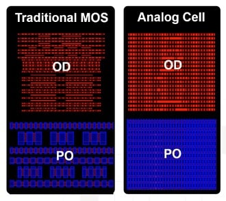
With this analog cell approach there is a uniform Oxide Diffusion (OD) and POlysilicon (PO), which improve silicon yields.

Automating Analog Cell Layout
By restricting the analog transistors inside of analog cells to use more regular patterns, then layout automation can be more readily used, like: automatic placement using templates, automatic routing with electrically-aware widths and spaces, and adding spare transistors to support any ECOs that arrive later in the design process.

Migrating between nodes the schematic topology is re-used, while the width and lengths per device do change. The APR settings are tuned for each analog component of a cell. APR constraints for analog metrics like currents and parasitic matching make this process smarter. To support an ECO flow, there’s an automatic spare transistor insertion feature. Both Cadence and Synopsys have worked with TSMC since 2021 to enable this improved analog automation methodology.
Migrating analog circuits to new process nodes requires a flow of device mapping, circuit optimization, layout re-use, analog APR, EM and IR fixes and post-layout simulations. During mapping an Id saturation method is used, where devices are automatically identified by their context.
Pseudo post-layout simulation can use estimates and some fully extracted values to shorten the analysis loop. Enhancements to IC layout tools from both Cadence and Synopsys now support schematic migration, circuit optimization and layout migration steps.
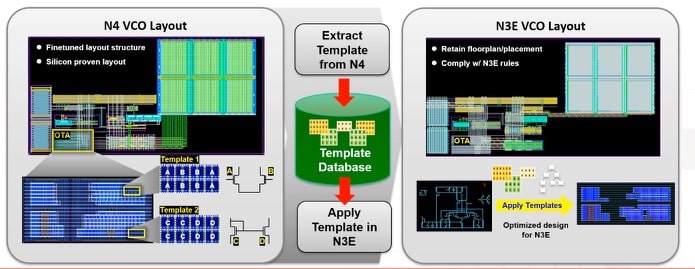
A VCO layout from N4 was migrated to the N3E node using automation steps and a template approach, reusing the placement and orientation of differential pair and current mirror devices. The new automated approach for migration was compared to a manual approach, where the time required for manual migration was 50 days and with automation only 20 days, so a 2.5X productivity improvement. Early EM, IR and parasitic RC checks was fundamental to reaching the productivity gains.

A ring-based VCO was also migrated both manually and automatically from the N40 to N22 node, using Pcells. The productivity gain was 2X by using the automated flow. Pcells had more limitations, so the productivity gain was a bit less.
Summary
TSMC has faced the challenges of analog cell migration by: collaborating with EDA vendors like Cadence and Synopsys to modify their tools, using analog cells with fixed heights to allow more layout automation, and adopting similar strategies to digital flows. Two migration examples show that the productivity improvements can reach 2.5X when using smaller nodes, like N5 to N3. Even with mature nodes like N40, you can expect a 2X productivity improvement using Pcells.
If you registered for the TSMC OIP, then you can watch the full 31 minute video online.
Related Blogs
- Samsung Versus TSMC Update 2022
- TSMC OIP – Enabling System Innovation
- TSMC Expands the OIP Ecosystem!
- TSMC 2022 Open Innovation Platform Ecosystem Forum Preview
- Three Key Takeaways from the 2022 TSMC Technical Symposium!


Comments
2 Replies to “TSMC OIP – Analog Cell Migration”
You must register or log in to view/post comments.