An update is now available here: Application-Specific Lithography: Patterning 5nm 5.5-Track Metal by DUV
The 5nm foundry (e.g., TSMC) node may see the introduction of 6-track cells (two double-width rails plus four minimum-width dense lines) with a minimum metal pitch in the neighborhood of 30 nm. IMEC had studied a representative case as its ‘7nm’ case [1]. TSMC had some published 5nm test structures which looked like extended 6-track cells [2]. Even with EUV lithography, the use of highly specialized patterning techniques is expected. We consider various options here for patterning the lines of the 6-track cell (Figure 1).
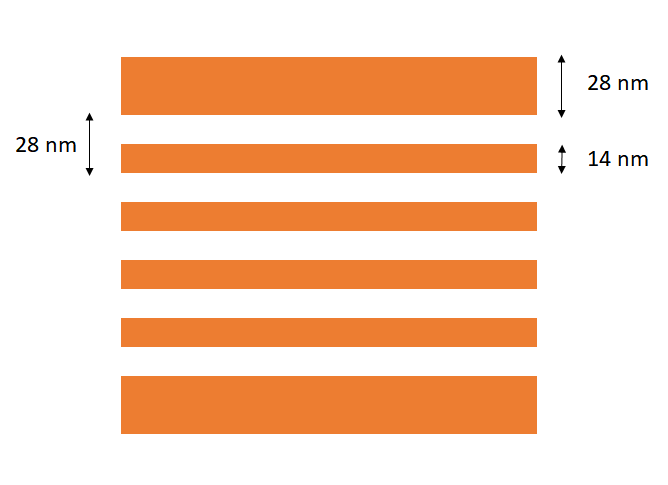
Figure 1. Reference example for 5nm 6-track cell with four 14 nm metal lines spaced 14 nm apart, and two 28 nm wide rails at the upper and lower boundaries.
Single Exposure EUV
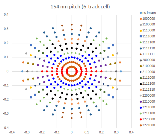
At first glance, a single exposure technique using EUV should be easiest to carry out without much yield consideration. However, EUV has many added concerns uncovered over the years such as stochastic variation [3-5]. Figure 2 shows the map of pupil sources correlated with the possible diffraction patterns for a 154 nm pitch 6-T cell (14 nm internal half-pitch, 28 nm rail width). Unfortunately, each individual diffraction pattern takes less than 20% pupil fill, leading to throughput loss for a dedicated diffraction pattern on the current NXE:3400B systems [6].
Figure 2. All possible diffraction patterns for a single EUV 0.33 NA exposure of the 6-track cell line pattern in Figure 1. Each different symbol represents a diffraction pattern produced by the corresponding EUV source point, labeled by a 7-digit string. The nth digit indicates how many -nth, nth orders are included (0, 1 or 2).
When the illumination is expected to spread the photon number over at least several diffraction patterns, each source point effectively becomes more noisy [5].
SAQP
A more familiar alternative, but not without its own technical challenges, is self-aligned quadruple patterning (SAQP), using immersion lithography. Conducting features are best defined between spacers to make cutting more efficient; this is also known as the “spacer-is-dielectric” (SID) approach [7]. The biggest hurdle is that the number of spacers is naturally even, so that the features defined between spacers will naturally come in odd numbers. As a workaround, some spacers may be made to disappear or merge, with a deliberately narrowed space between some starting features. Effectively, this removes one spacer to leave an odd number of spacers, with an even number of features in between. For the 154 nm pitch case being studied, the starting pattern proposed in [1] could actually be drawn as a 308 nm pitch pattern as shown in Figure 3.
Figure 3. SAQP integration for 6-track cell. Blue: starting (core or mandrel) features. Green: 1st spacer. Red: 2nd spacer. Purple: dielectric masked by 2nd spacer. Gray: metal filling in between spacers. In some schemes, the material filled at the 1st spacer locations is different from that filled at other locations between the 2nd spacers. This is to facilitate self-aligned blocking [1].
Pitch Walking
Due to the breaking of symmetry in the pattern of Figure 1, “pitch walking” is likely to occur in the patterning process. This is the effect where the spacing between some lines is decreased or increased relative to the spacing between other lines. This can occur in the lithography process itself, due to defocus, for either the EUV or SAQP options described above.
For the EUV case, the different illumination source points can produce different effects (Figure 4). This is again aggravated by stochastic sensitivity.
Figure 4. Defocus can cause pitch walking to an extent dependent on the source points for illumination. The conditions assumed for this 6-track cell example are 154 nm pitch, 13.5 nm wavelength, 0.33 NA, 50 nm defocus.
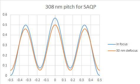
For the SAQP case, there are additional potential contributors to pitch walking from process steps following the lithography, such as spacer deposition thickness and spacer overetch. These extra conditions force tighter tolerances on defocus for the starting features, so that even 30 nm could be limiting (Figure 5).
Figure 5. For SAQP, defocus tolerance needs to be tighter to prevent pitch walking caused by post-litho process steps.
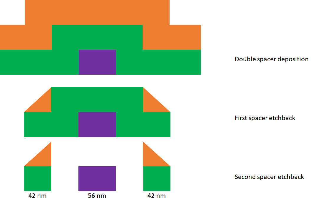
A potential mitigation of the defocus impact is to use a multi-patterning technique instead of a symmetry-breaking single exposure for the SAQP starting features. In the most brute-force case, 3 exposures, 3 etches may be used to each pattern one of the three starting features (the central 56 nm and the two side 42 nm features) within the 308 nm pitch. A more efficient way would be to use self-aligned triple patterning (SATP) [8] to define all three features with one mask (Figure 6). For this process, the lithography will maintain repeating feature symmetry.
Figure 6. SATP flow [8] using two spacers for producing the starting features for SAQP shown in Figure 3.
Other steps that can be taken to address pitch walking for SAQP include thickness optimization [9] and process control loop feedback [10]. Presumably, the same issues have been encountered for self-aligned double patterning (SADP) already, so as SADP matures, SAQP should benefit.
Self-aligned blocking or cutting
The breaks in the line tracks also need to be patterned. Within the same EUV exposure as the lines, the extra pitches in the second dimension create more diffraction patterns among which the EUV photon number will be divided [5], further aggravating the stochastic effects. Line ends are already small collection areas for photons [11], leading to extra tip-to-tip variation. The classical resolution limit for line end gaps is ~ 0.6 wavelength/NA [12], where NA is the numerical aperture of the lithography system (~25 nm for the NXE:3400 with 0.33 NA). Thus, a separate exposure for cutting the lines, or blocking the etch at some locations, is preferred.
The self-aligned block (SAB) approach is preferred over a single exposure block or cut, due to its being more robust against overlay and edge placement errors [1,13]. However, the SAB approach necessitates the use of two masks, as two oppositely selective etches will be used for different block/cut locations. While EUV is commonly discussed for use in the SAB approach, immersion lithography can also be used, with self-aligned double patterning (SADP) as needed [14].
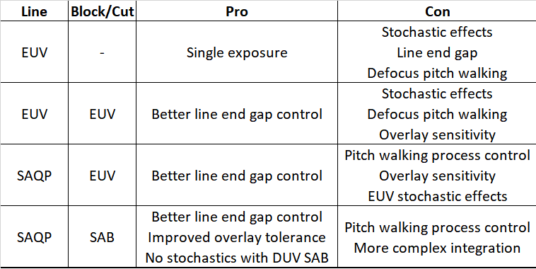
Summary of approaches
The pros and cons of the approaches covered above are summarized in the table below:
References
[1] J. U. Lee, S. H. Choi, Y. Sherazzi, R. R. H. Kim, “SAQP spacer merge and EUV self-aligned block decomposition at 28nm metal pitch on imec 7nm node,” Proc. SPIE 10962, 109620N (2019).
[2] G. Yeap, S. S. Lin, Y. M. Chen, H. L. Shang, P. W. Wang, H. C. Lin, Y. C. Peng, J. Y. Sheu, M. Wang, X. Chen, B. R. Yang, C. P. Lin, F. C. Yang, Y. K. Leung, D. W. Lin, C. P. Chen, K. F. Yu, D. H. Chen, C. Y. Chang, H. K. Chen, P. Hung, C. S. Hou, Y. K. Cheng, J. Chang, L. Yuan, C. K. Lin, C. C. Chen, Y. C. Yeo, M. H. Tsai, H. T. Lin, C. O. Chui, K. B. Huang, W. Chang, H. J. Lin, K. W. Chen, R. Chen, S. H. Sun, Q. Fu, H. T. Yang, H. T. Chiang, C. C. Yeh, T. L. Lee, C. H. Wang, S. L. Shue, C. W. Wu, R. Lu, W. R. Lin, J. Wu, F. Lai, Y. H. Wu, B. Z. Tien, Y. C. Huang, L. C. Lu, J. He, Y. Ku, J. Lin, M. Cao, T. S. Chang, S. M. Jang, “5nm CMOS Production Technology Platform featuring full-fledged EUV, and High-Mobility Channel FinFETs with densest 0.021 um2 SRAM cells for Mobile SOC and High Performance Computing Applications,” IEDM 2019.
[3] A. Frommhold, D. Cerbu, J. Bekaert, L. Van Look, M. Maslow, G. Rispens, E. Hendrickx, “Predicting Stochastic Defects across the Process Window,” Proc. SPIE 11147, 1114708 (2019).
[4] P. De Bisschop, E. Hendrickx, “Stochastic Printing Failures in EUV Lithography,” Proc. SPIE 10957, 109570E (2019).
[5] https://www.linkedin.com/pulse/stochastic-variation-euv-source-illumination-frederick-chen/
[6] M. van de Kerkhof, H. Jasper, L. Levasier, R. Peeters, R. van Es, J-W. Bosker, A. Zdravkov, E. Lenderink, F. Evangelista, P. Broman, B. Bilski, T. Last, “Enabling sub-10nm node lithography: presenting the NXE:3400B EUV scanner,” Proc. SPIE 10143, 101430D (2017).
[7] Y. Ban, D. Z. Pan, “Self-aligned double-patterning layout decomposition for two-dimensional random metals for sub-10-nm node design,” J. Micro/Nanolith. MEMS MOEMS 14, 011004 (2014).
[8] J-Y. Lee, J-S. Park, S-G. Woo, US Patent 7842601, assigned to Samsung, filed Apr. 20, 2006.
[9] T. Yang, D. Yim, “SAQP Pitch walking improvement pathfinding by simulation,” 41st International Symposium on Dry Process, 2019. http://www.dry-process.org/2019/poster_program.html
[10] H. Ren, A. Mani, S. Han, X. Li, X. Chen, D. Van Den 90Heuvel, “Advanced process control loop for SAQP pitch walk with combined lithography, deposition and etch actuators,” Proc. SPIE 11325, 1132523 (2020).
[11] https://www.linkedin.com/pulse/photon-shot-noise-impact-line-end-placement-frederick-chen/
[12] https://www.linkedin.com/pulse/lithography-resolution-limits-line-end-gaps-frederick-chen
[13] A. Raley, N. Mohanty, X. Sun, R. A. Farrell, J. T. Smith, A. Ko, A. W. Metz, P. Biolsi, A. Devilliers, “Self-Aligned Blocking Integration Demonstration for Critical sub 40nm pitch Mx Level Patterning,” Proc. SPIE 10149, 101490O (2017).
[14] E.g., see A. J. deVilliers, US Patent 9240329, assigned to Tokyo Electron Limited, filed Feb. 17, 2015.
The original article first appeared in LinkedIn Pulse: Application-Specific Lithography: The 5nm 6-Track Cell






Musk’s Orbital Compute Vision: TERAFAB and the End of the Terrestrial Data Center