

 I came across an interesting article by Will Strauss which is pretty much the history of DSP in communication chips. Having lived through the early part of the history while I was at VLSI Technology I found it especially interesting.
At VSLI, our first GSM (2G, i.e. digital not analog air interface) was a 5-chip chipset. The DSP functionality was all hard-coded since I don’t think in that era there were any licensable DSP cores that had enough power. As usual when a new communications standard is first implemented (think LTE today, or gigabit Ethernet if that is your thing) it is right on the edge of what is implementable in the silicon technology of the day. Nobody wants a standard that is lower performance than necessary, and which will inevitably be superseded by a higher performance standard as silicon performance improves. After all, we’d all love terabit downloads to our smartphones if we knew how to build them, it is not the standardization process that is the limiting factor, it is mostly just raw semiconductor technology performance (and power). I am not even sure if the DSP functionality was even coded in RTL, that was the era when synthesis was just going mainstream. It might still have been schematics.
This 5-chip chipset was reduced to two chips and then to one. But the tradeoffs between hardware and software were changing. It was attractive to use a programmable (in assembly) DSP core instead of writing RTL (and especially instead of drawing schematics!). VLSI licensed Pine and Oak from DSP Group, one of the ancestors of today’s CEVA. DSP Group had originally developed their own DSP cores primarily, I believe, for building tapeless telephone answering machines (remember them?). But they also licensed the cores to other companies, following the model that ARM had started to use. Later VLSI also licensed the higher performance Teak core for CDMA chipsets (which required about 100 MIPS of DSP performance, much more than GSM).
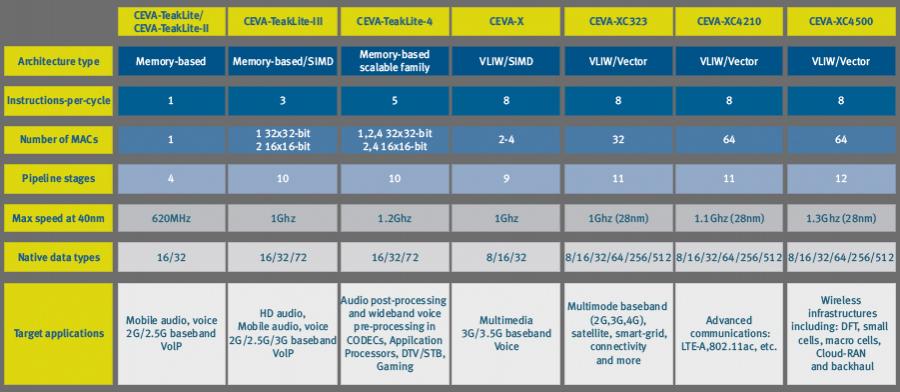
Today, nobody in their right minds would consider building a state-of-the-art LTE modem by sitting down with a text editor and writing RTL. The only approach is to either build a DSP (as Qualcomm and nVidia have done) or license one (as Samsung and Mediatek have done). CEVA are the market leaders in DSP in general and DSP for communications SoCs in particular). Plus another change is that nobody in their right minds would think of programming a modern DSP in assembly. This is not your father’s DSP: it is multiple issue VLIW instruction-set with dozens of MACs and other vector units all operating in parallel. There is no way to program something like that by hand. Creating the software toolchain for a DSP (compilers, debuggers, models etc) is just as important as creating the netlist.
 Will Strauss’s article covers the same process as we went through at VLSI and brings it up to the present day. One big trend in smartphone SoCs is the move to integrate the modem (and thus the DSP) onto the application processor and thus also make it available for specialist use for non-modem functionality such as image processing. Apple currently is going against this trend, the Ax SoCs are designed to work with Qualcomm modems. But the Qualcomm Snapdragon chips have both functions integrated, as does Mediatek, and the low-end smartphone market largely uses these chips.
But to emphasize just how daunting it is to build a state of the art modem like this from scratch, without licensing a whole substem from someone like CEVA, look at Intel. Even they, after their acquisition of Infineon Wireless, struggled to build their own and had to buy Fujitsu’s LTE modem group to get the job done and as far as I know still haven’t managed to build one that runs in their own 22nm FinFET process.
Once again the Will Strauss article is here. The CEVA website is here.
More articles by Paul McLellan…


Comments
There are no comments yet.
You must register or log in to view/post comments.