As AI, HPC, and networking applications demand ever-higher compute and bandwidth, SoC complexity continues to grow. Traditional 50M ASIC equivalent gate FPGA prototyping systems have become less effective for full-chip verification at scale. Addressing this challenge, S2C introduced the Prodigy S8-100 Logic system, powered by AMD’s Versal™ Premium VP1902, offering 2× performance and enhanced deployment efficiency for ultra-large SoC designs.
S8-100 vs. LX2 Benchmark
S2C ran a head-to-head benchmark using the Openpiton 192Core project—a highly complex, multi-core SoC design. This comparison evaluated the performance of the VP1902-based S8-100Q against the previous generation LX2 platform across key prototyping metrics:
| Metric | S8-100Q (4× VP1902) | LX2 (8× VU19P) | S8-100 Advantage
|
| Design Size (Total) | 268.74M gates
(based on usage) |
249.02M gates
(based on usage) |
✔ Same design workload |
| Cut Size | 25,002 | 54,990 | ✔ Simplified topology |
| Post-PR Frequency (MHz) | 9.4 | 4.6 | ✔ 2× performance |
Despite equivalent logic capacity, the S8-100Q achieved 2× higher operating frequency, reduced cascading complexity, and minimized design constraints—leading to faster bring-up and more efficient debug cycles.
Test Conditions:
- S2C PlayerPro-CT 2024.2 via fully automated, timing-aware partitioning
- Xilinx Vivado 2024.2 for synthesis and implementation
- Global optimization techniques enabled, including TDM-awareness, clock domain balancing, and resource co-optimization
Performance Advantages
1) Architecture Enhancement
- Delivers ~2× logic density
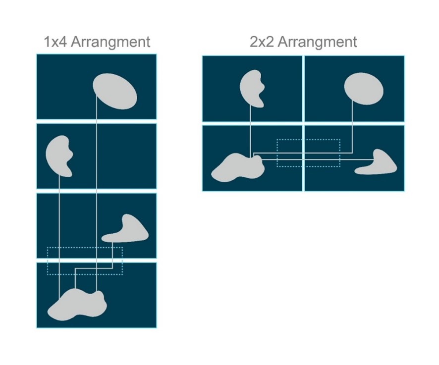
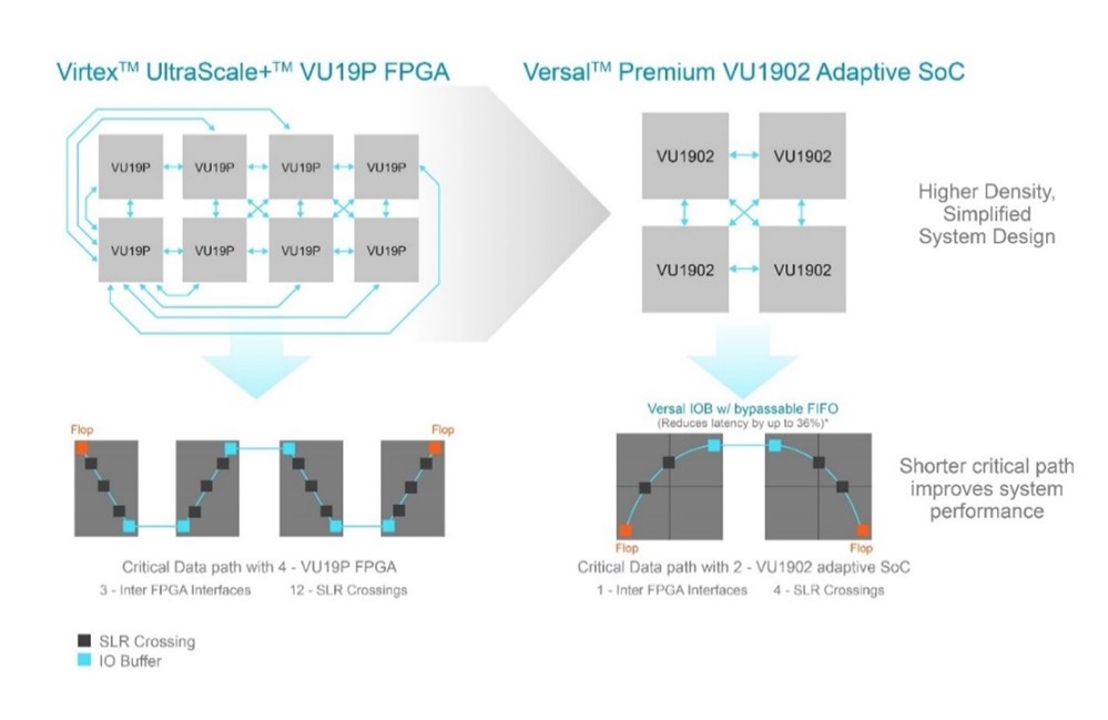
- 2×2 die layout reduces longest possible signal path from 3 to 2 hops—improving timing closure

2) Streamlined Partitioning & Cascading
- Higher per-FPGA capacity reduces chip-to-chip interconnects
- Fewer SLR crossings minimize congestion and simplify routing
3) Low-Latency Interconnect Fabric
- I/O latency is reduced by 36% of that in UltraScale+ systems

Smarter Prototyping with Integrated Toolchains
The S8-100 isn’t just powerful—it’s intelligently automated. S2C’s PlayerPro-CT toolchain tightly integrates with the hardware, offering:
- One-click flow from RTL to bitstream
- Optional manual refinement for advanced tuning
- Timing and Architecture-aware optimizations
The combination of the S8-100 and new PlayerPro-CT features dramatically cuts setup time, boosts resource efficiency, and accelerates project time-to-market.
Field-Tested and Deployment-Ready
The S8-100 has been deployed in advanced-node SoC programs across AI acceleration, edge computing, and data center. Its proven performance, scalable architecture, and reduced engineering overhead make it a trusted choice for complex SoC projects.
With 2× logic density, simplified interconnects, and a tightly integrated toolchain, the S8-100 delivers a major leap forward in FPGA-based prototyping—empowering engineering teams to confidently prototype, validate, and iterate faster than ever before.
For more information, please visit: www.s2cinc.com.
About S2C
S2C is a global leader in FPGA prototyping solutions, providing scalable, reliable, and flexible hardware platforms that accelerate system validation and software development for semiconductor companies worldwide. For more information, visit www.s2cinc.com.
Also Read:
Cost-Effective and Scalable: A Smarter Choice for RISC-V Development
S2C: Empowering Smarter Futures with Arm-Based Solutions
Share this post via:


Comments
There are no comments yet.
You must register or log in to view/post comments.