In today’s rapidly advancing technological landscape, semiconductors are at the heart of innovation across diverse industries such as automotive, healthcare, telecommunications, and consumer electronics. As a leader in technology and engineering, Siemens plays a pivotal role in empowering the next generation of designs with its integrated approach to system design. This fact may sometimes get drowned in a torrent of others news, particularly when people don’t hear the decades old familiar name “Mentor Graphics” in the news anymore. Siemens retired that name in 2021 and replaced it with Siemens EDA, a segment of Siemens Digital Industries Software. Siemens EDA’s financials are not separately disclosed publicly as when Mentor Graphics was a separate company. Naturally, there are lots of questions in people’s minds about Siemens EDA’s role within the broader ecosystem, how it is performing and where it is headed.
At the recent User2user conference, Mike Ellow, Siemens EDA’s Executive Vice President gave an excellent keynote talk that addressed all these questions and more. His talk provided insights into how Siemens EDA is doing, its vision, its key investment areas and why Siemens EDA is an investment priority at Siemens. The following is a synthesis with some excerpts from Mike’s keynote presentation.
How is Siemens EDA Doing?
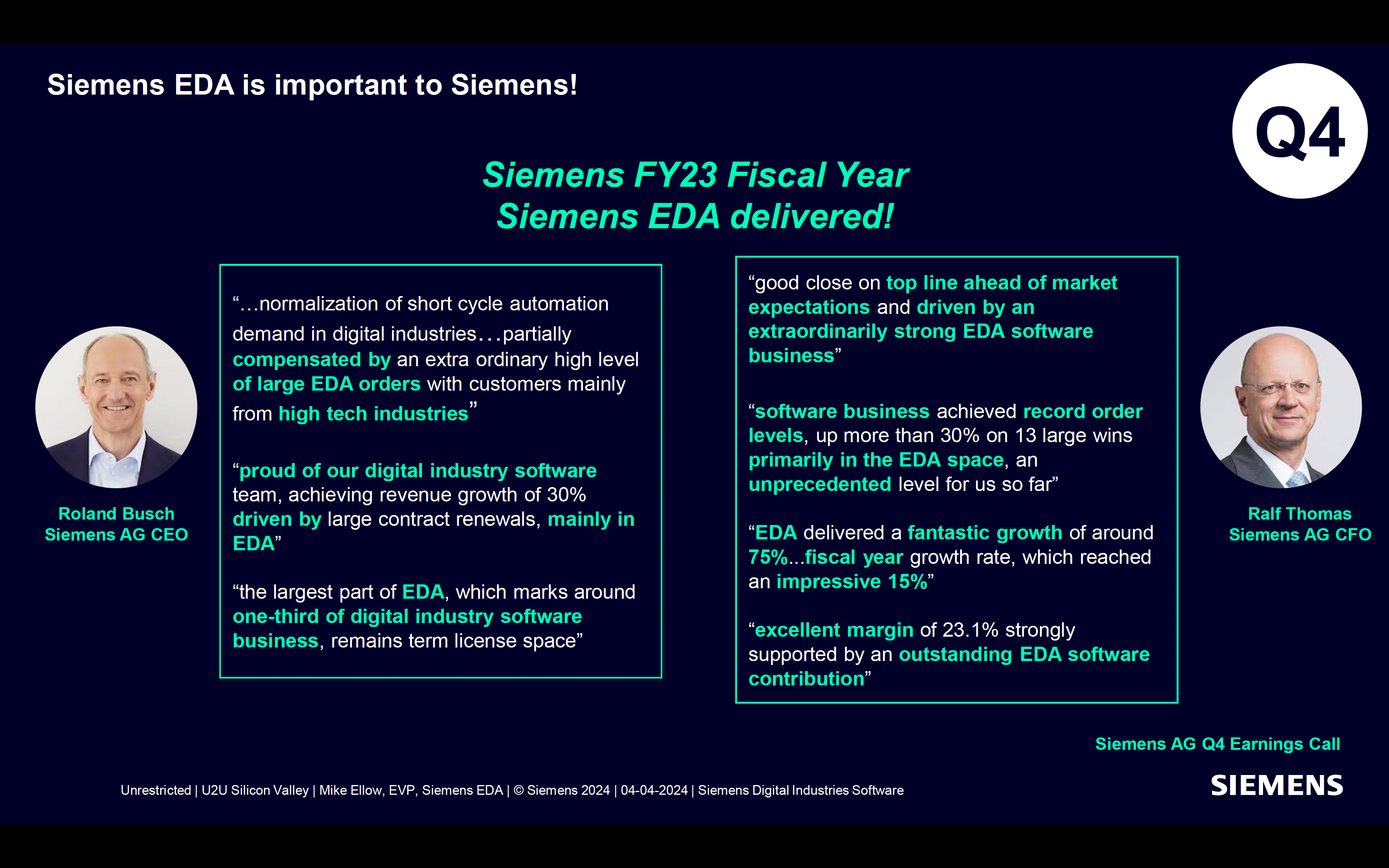
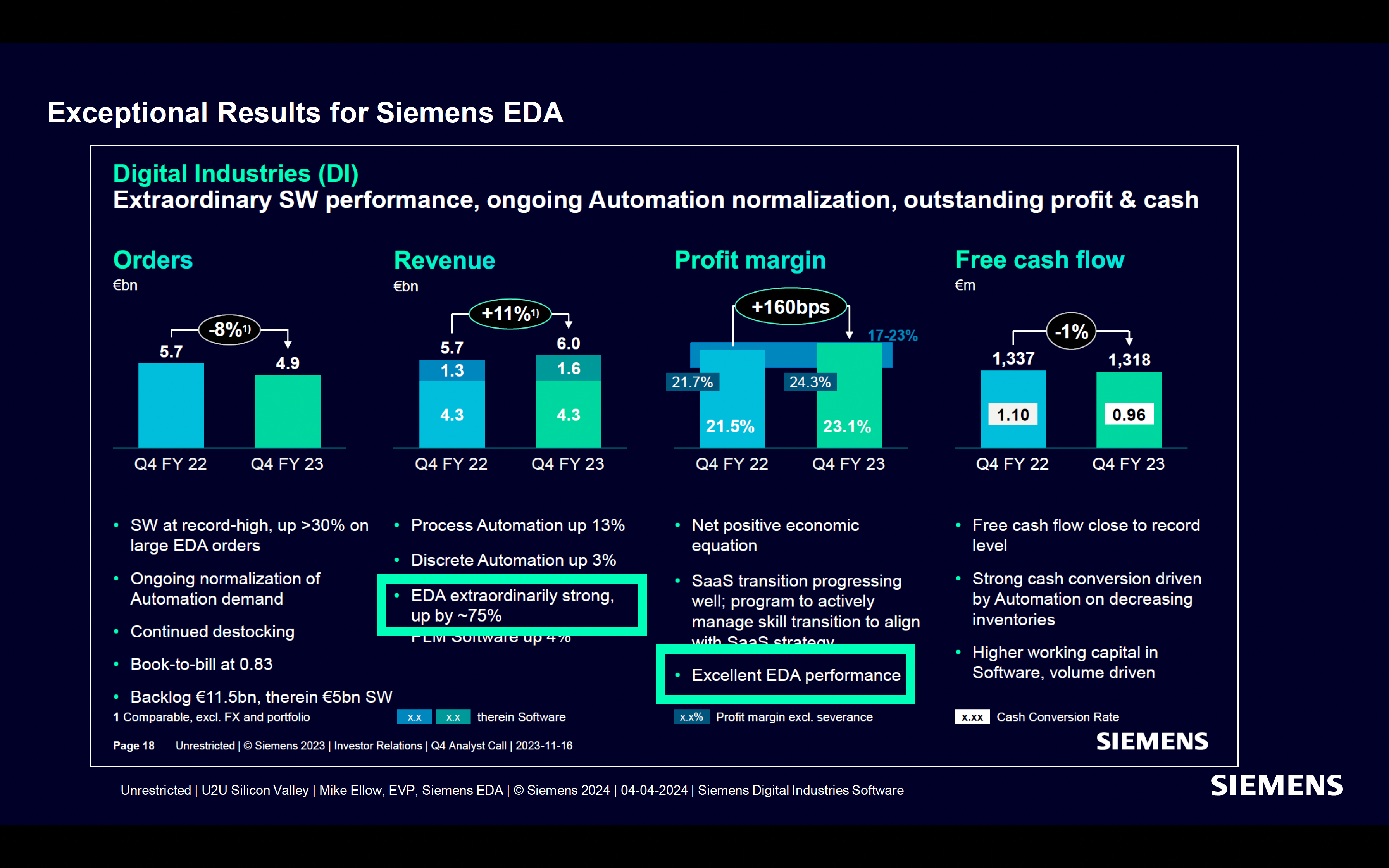
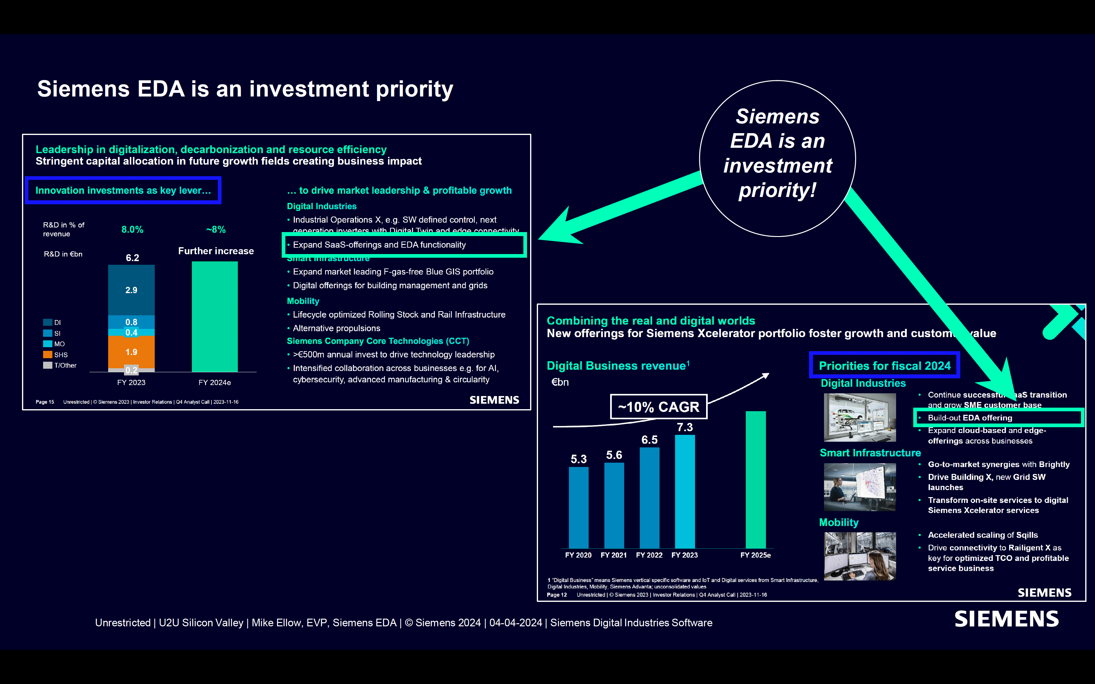
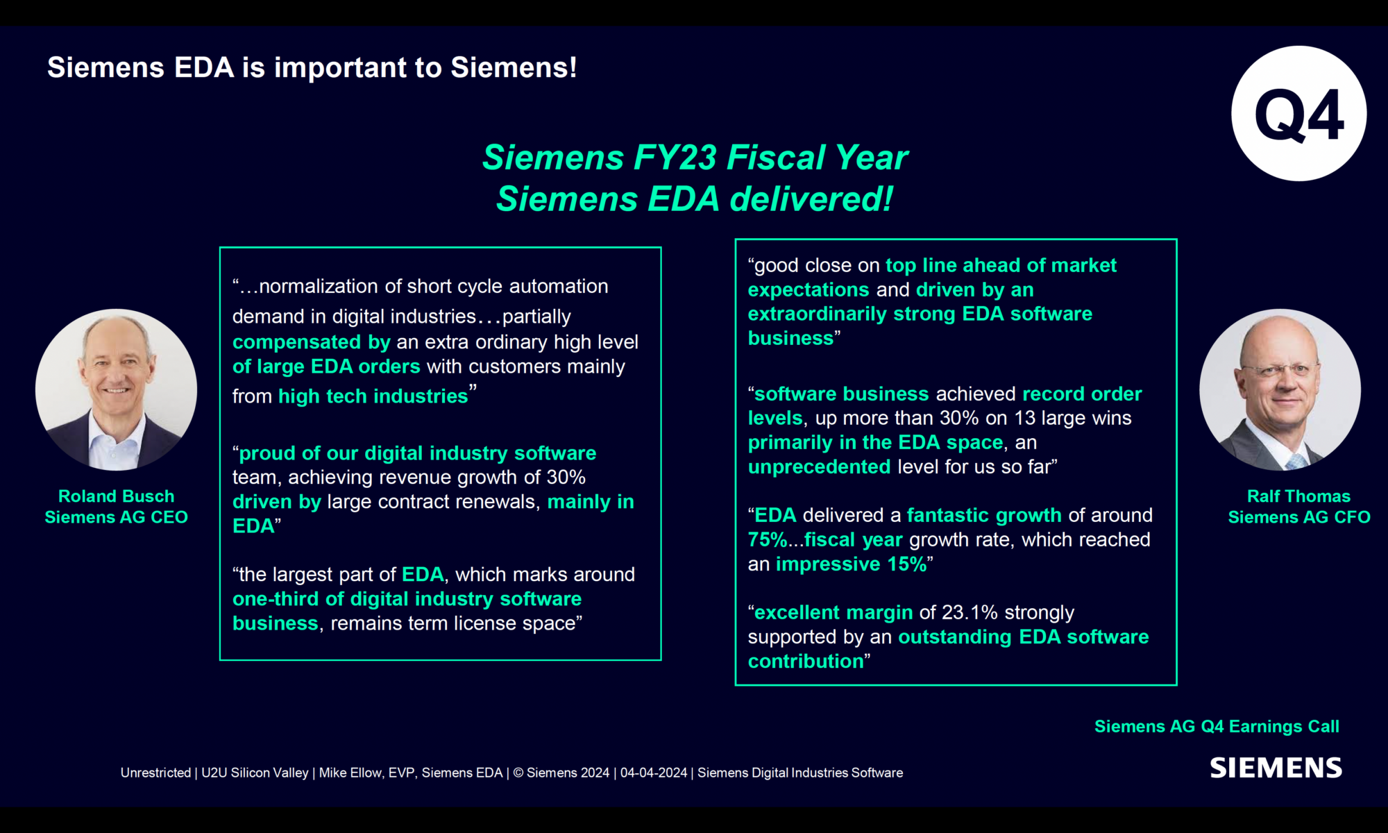
Siemens EDA demonstrated its EDA leadership through its 14% year-on-year growth in their recently closed fiscal year. This is noteworthy given Siemens EDA’s revenue does not include any significant IP revenue stream. The division also experienced a double-digit percentage increase in R&D headcount, which is the highest investment in Siemens EDA’s history (excluding acquisitions).
The following charts provide more financial details and speak for themselves.
Why is Siemens Investing in Siemens EDA?
We in the semiconductor and electronics industries have always known that semiconductors are at the center of a changing world. The only difference now is that everyone else has recognized it too.

![]()
And the semiconductor industry is projected to grow at an incredibly accelerated pace, crossing $1 trillion by 2030 [Sources: International Business Strategies/Nov 2022 and VLSI Research/Dec 2022].
Siemens EDA Enabling A New Era for System Design
Siemens EDA’s comprehensive digital twin technology plays a critical role in the design, verification, and manufacturing of complex electronic systems. A digital twin is a virtual representation of a physical system or product, and in the context of electronic design automation (EDA), it encompasses various aspects of electronic system development. Siemens EDA focuses on three key investment areas that enhance the capabilities of Siemens EDA’s digital twin technology, providing an integrated, holistic approach to design, verification, and manufacturing.
Accelerated System Design:
Leveraging advanced tools and methodologies to speed up the design process, accelerated system design includes high-level synthesis, system-level design and verification, and virtual prototyping. These tools enable engineers to quickly model and simulate complex electronic systems, leading to faster time-to-market and improved quality.
Advanced Heterogeneous Integration:
Combining different types of components and technologies on a single package or substrate, advanced heterogeneous integration facilitates the development of highly integrated and compact systems. Siemens EDA’s solutions include 3D ICs, multi-die packaging, and advanced packaging and assembly.
Manufacturing-Aware Advanced Node Design:
This area involves creating electronic designs that take into account the intricacies of advanced manufacturing processes. Design for manufacturability (DFM), process technology co-design, and support for advanced node technologies enable engineers to create optimized designs that can be reliably manufactured.
Revolutionizing Electronic System Design
Some key solutions that Mike touched upon during his keynote talk include:
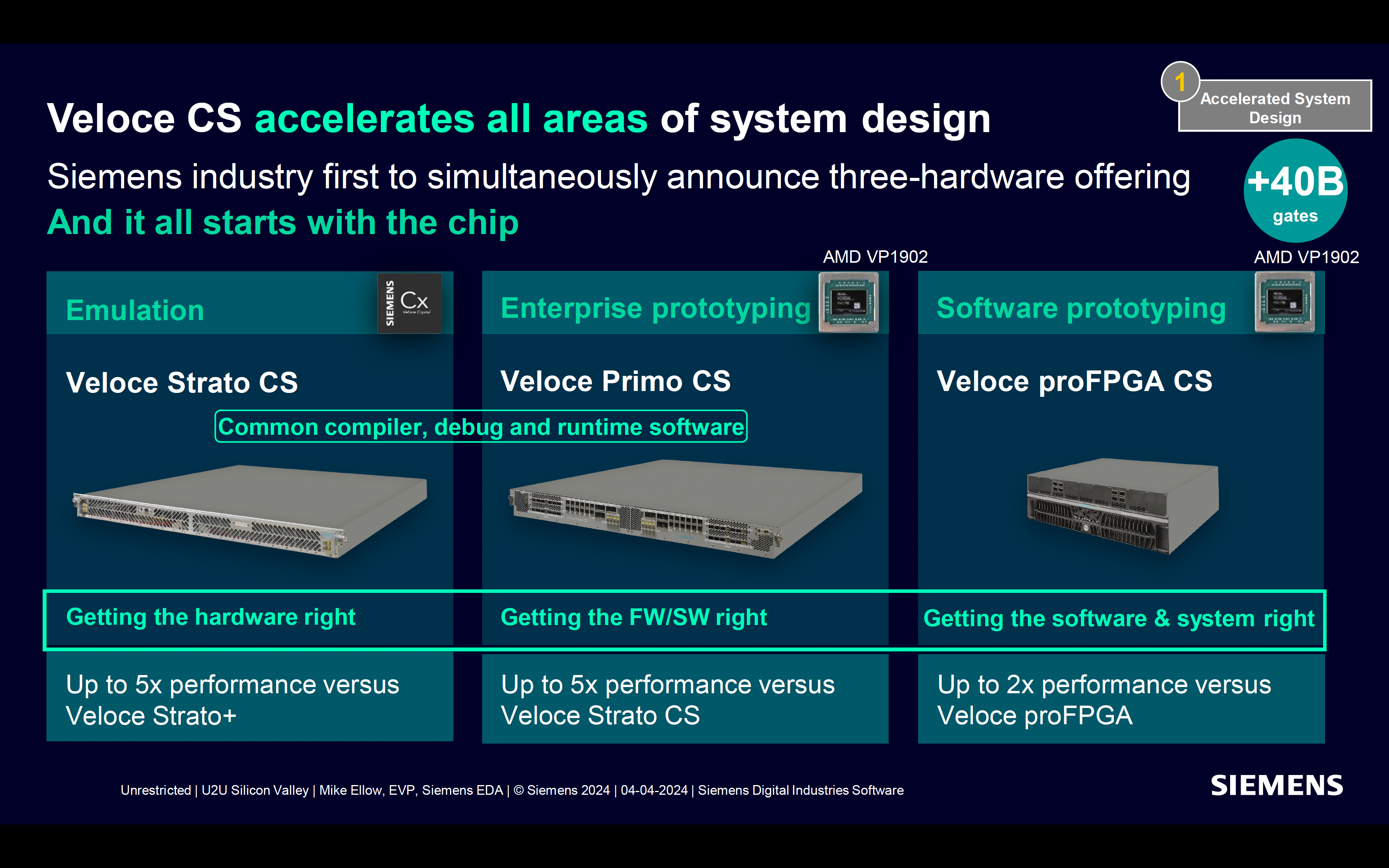
Veloce CS Accelerates All Areas of System Design
Recently announced Siemens EDA’s Veloce CS platform offers high-speed emulation and prototyping capabilities, accelerating the verification of complex electronic systems. Veloce CS streamlines design, verification, and testing processes, enhancing overall product development efficiency. At 40B gates capacity, the solution boasts the highest capacity solution in the industry. Key features include:
Early Software Development: Veloce CS provides a hardware platform for early software development, allowing software teams to test and debug their code on virtual hardware.
Full-System Simulation: Engineers can simulate entire systems, including hardware, software, and peripherals, to ensure all aspects of the design work together seamlessly.
Comprehensive Debugging: Advanced debugging features such as waveform viewing, performance profiling, and hardware-assisted tracing help engineers identify and resolve issues quickly.
3DIC Tooling
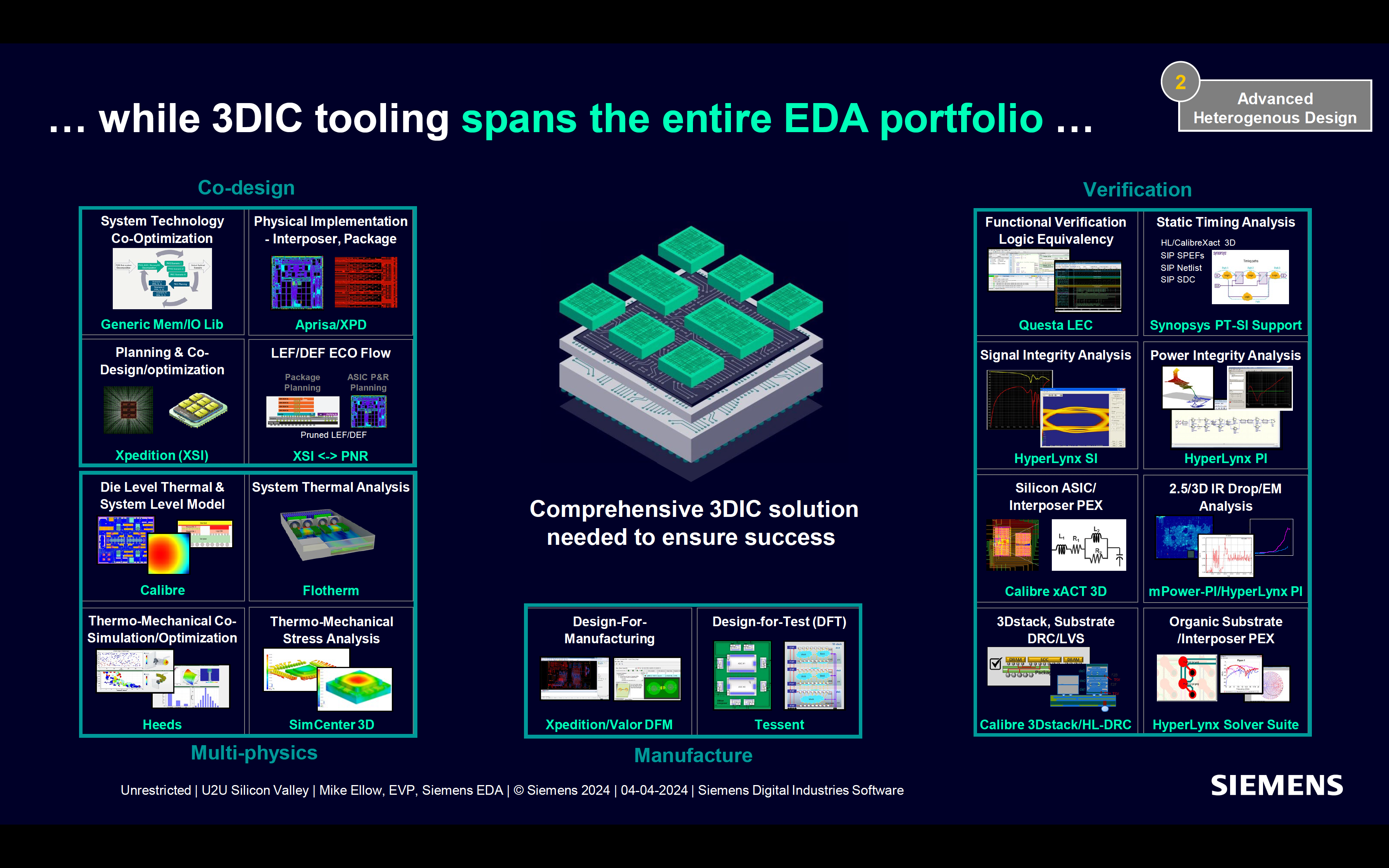
Siemens EDA’s 3D integrated circuit (3DIC) tooling spans its entire portfolio, providing comprehensive support for the design, verification, and manufacturing of 3DICs. This includes:
Design Tools: Siemens EDA offers tools for floorplanning, partitioning, and routing 3DIC designs to optimize performance and space usage.
Verification and Simulation: Advanced tools for simulating power, thermal, and signal integrity aspects of 3DICs ensure reliable performance.
Physical Implementation: 3DIC layout and design for manufacturability (DFM) tools help create detailed designs that can be manufactured efficiently.
3DIC Modeling and Visualization: Engineers can use advanced modeling and visualization tools to better understand spatial relationships and optimize designs.
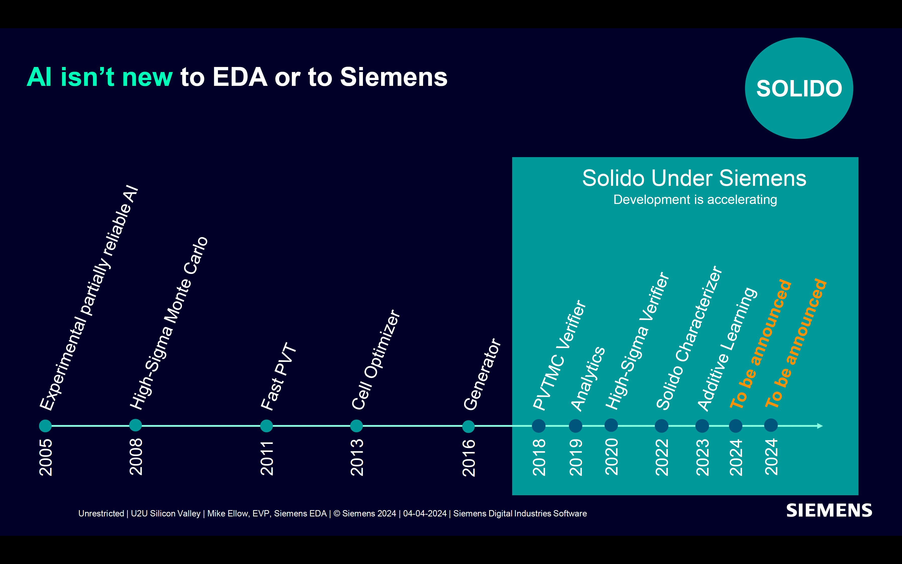
Solido Statistical Analysis and Optimization
Solido is a technology suite focusing on the design, verification, and optimization of integrated circuits (ICs) using advanced statistical analysis and machine learning techniques, especially in the context of process variability. Solido’s tools allow engineers to handle the complexities of modern IC design, creating reliable, high-quality designs.
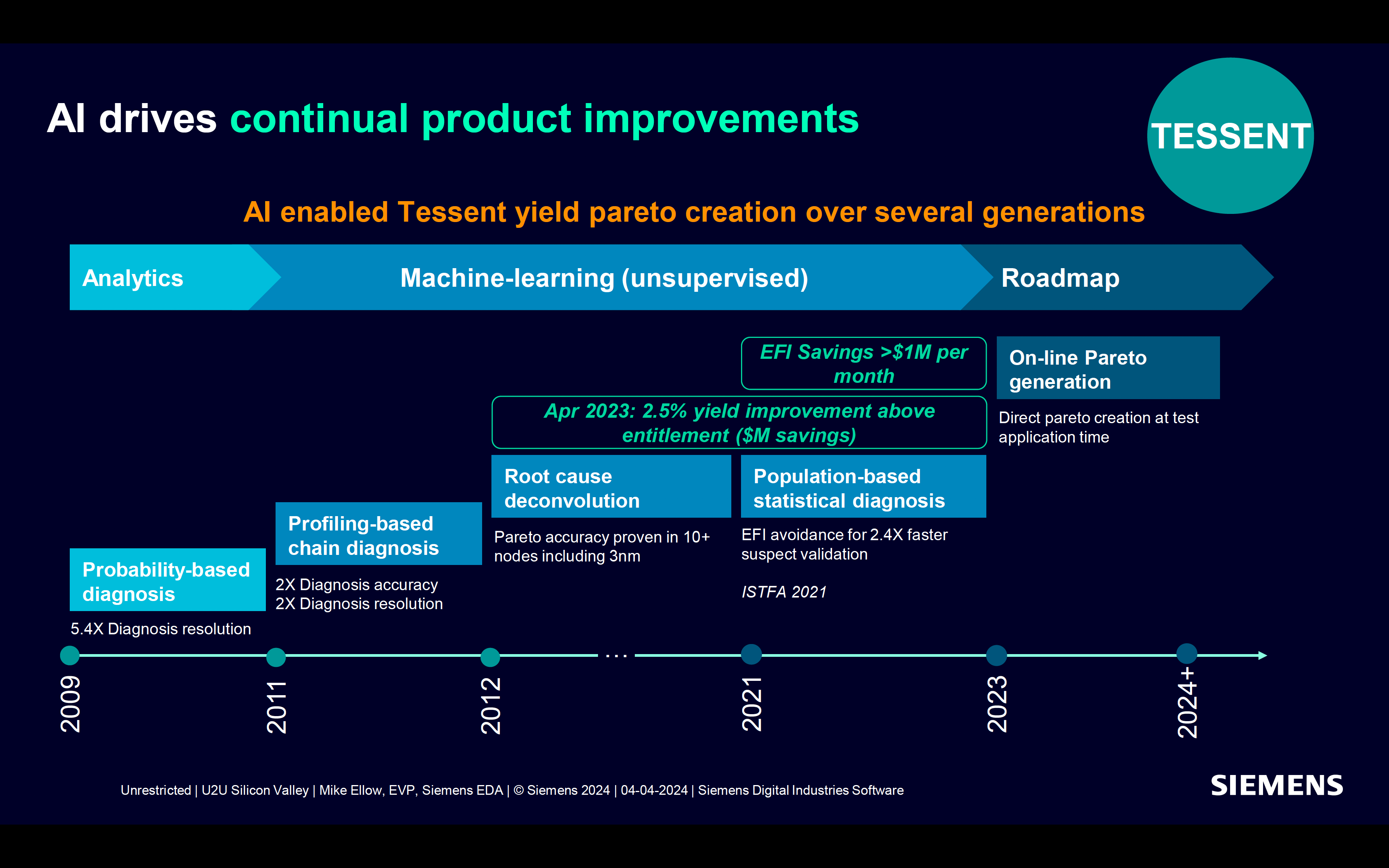
Tessent Embedded Analytics
Siemens EDA Tessent offers a suite of tools for design-for-test (DFT), design-for-diagnosis (DFD), and design-for-reliability (DFR) in semiconductor devices. These solutions improve testability, diagnosis, and reliability in electronic designs, contributing to the creation of high-quality, functional semiconductor devices.
Artificial Intelligence (AI) not new to Siemens EDA
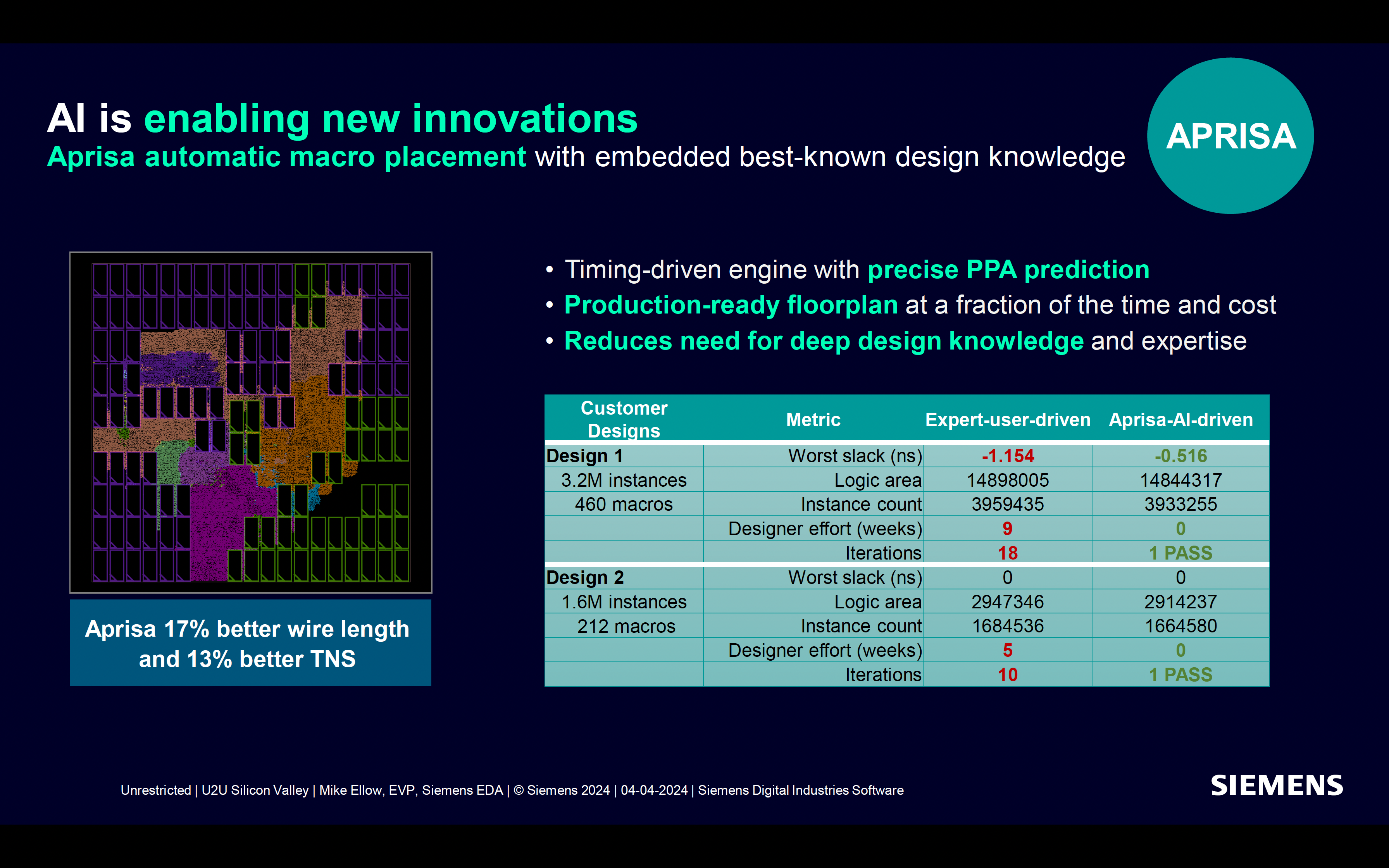
Siemens EDA has been leveraging AI for many years well before AI became a buzz word in the industry, through its products such as Solido and Tessent. Now of course, AI techniques are being leveraged by products across its entire EDA portfolio.
Summary
Siemens EDA’s integrated approach to system design, combined with its comprehensive EDA solutions, positions the company as a leader in enabling imagination and driving innovation in the semiconductor industry. Through early software validation, manufacturing-aware design, AI-enhanced design automation tooling, open ecosystem enablement, and advanced EDA tools, Siemens EDA is empowering engineers and designers to create the next generation of high-quality, leading-edge systems. As technology continues to evolve, Siemens EDA’s solutions will play a crucial role in shaping the future of electronics and ensuring continued success for its customers and the wider industry.
Also Read:
Design Stage Verification Gives a Boost for IP Designers
Checking and Fixing Antenna Effects in IC Layouts
Siemens Promotes Digital Threads for Electronic Systems Design
Share this post via:


Comments
There are no comments yet.
You must register or log in to view/post comments.