As described in DO-254, any inability to verify specific requirements by test on the device itself must be justified, and alternative means must be provided. Certification authorities favor verification by test for formal verification credits because of the simple fact that hardware flies not simulation models. Requirements… Read More
 Arteris Highlights a Path to Scalable Multi-Die Systems at the Chiplet SummitAt the recent Chiplet Summit, presentations, discussions and…Read More
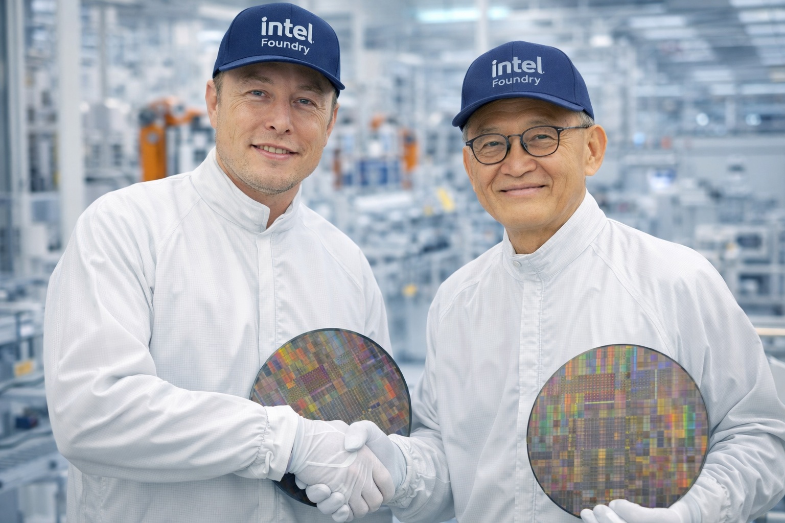 Captain America: Can Elon Musk Save America's Chip Manufacturing Industry?Intel has posted three consecutive years of falling…Read More
 WEBINAR: Reclaiming Clock Margin at 3nm and BelowAt 3nm and below, clock networks have quietly…Read More
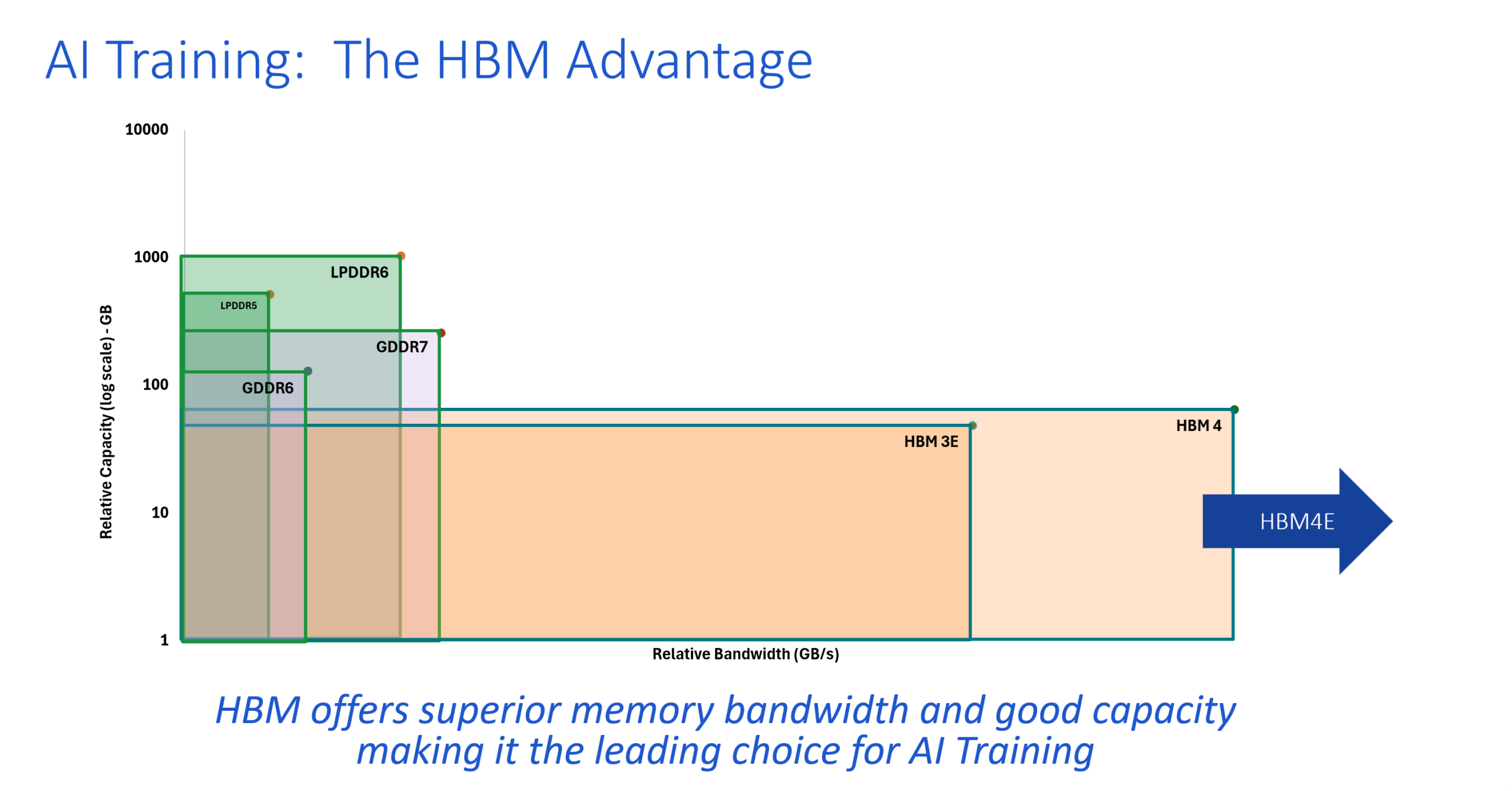 WEBINAR: HBM4E Advances Bandwidth Performance for AI TrainingThe rapid proliferation of LLMs and other AI…Read More
 Siemens Wins Best in Show Award at Chiplet Summit and Targets Broad 3D IC Design EnablementThe recent Chiplet Summit in Santa Clara was…Read More
Jasper User Group
The Jasper User Group meeting has been announced. It will take place on November 12th and 13th. As last year, it will be at the Cypress Hotel at 10050 De Anza Boulevard in Cupertino. The user group meeting is free for qualified Jasper customers.
Topics to be covered are, of course, all things verification:
- SoC subsystems verification
CEVA DSP Technology Symposium Series 2012
You are cordially invited to register to attend the CEVA DSP Technology Symposium Series 2012, which will take place in Taiwan, October 16th, China, October 18th and Israel, November 1st.
CEVA’s industry-leading experts and engineers will present a full day of lectures and seminars where you will learn about the latest technological… Read More
Chip Aware System Design
On Wednesday this week Ansys/Ansoft/Apache are presenting a new webinar Chip Aware System Design. It is presented by Dr Steven Gary Pytel Jr of the Ansoft part of Ansys, and Matt Elmore of the Apache subsidiary. The topics that will be covered include:
- Power Delivery Network (PDN) design requirements
- ABCD Matrix theory
- SYZ Matrix
SAME 2012 Conference on October 2-3 in Sophia is coming soon!
This is the 15[SUP]th[/SUP] anniversary for the SAME Conference, dedicated to innovation on Microelectronics. Sophia-Antipolis is not only close to Mediterranean sea, but also at the heart of Telecom valley in south of France, with Texas Instruments design center dedicated to Application Processor design (OMAP), Cadence… Read More
A Brief History of Helic
As I have mentioned before, you can tell al lot about a company by their CEO. The previous trip I made to Taiwan was with Helic co-founder and CEO Dr. Yorgos Koutsoyannopoulos. One of the benefits of my job is I get to spend time with some very interesting people from around the world and this was no exception.
Prior to founding Helic, … Read More
Taiwan Travel Explained!
Whenever people hear that I travel internationally one week a month they cringe at the thought of crowded airports, 12 hour flights, jet lag, and days packed with meetings. I generally shrug, accept the label of travel warrior, and say it is all part of doing business in the semiconductor ecosystem. But in reality, it is not as bad … Read More
Cadence Mixed Signal Technology Summit
Yesterday I attended some of the Cadence mixed-signal technology summit. The day ended with a panel session on Are We Closing the Gap Yet in Mixed-signal Design? Richard Goering moderated. The panelists were all mixed signal experts:
- Nayaz Khan of Maxim
- Nishant Shah of Broadcom
- Shiv Sikand of IC Manage
- Bill Meier of Texas Instruments
Atrenta Wins Gold
What is the most read article on design on EE Times website? Brian Bailey has an article up running through the top 10. It turns out that the #1 article is Understanding Clock Domain Issues by Saurabh Verma and Ashima S. Dabare of Atrenta. It actually had more than double the views of the second place paper. Checking clock domain crossing… Read More
The End of an Era
I drove down from San Francisco, where I live, to Silicon Valley this morning. Something odd was going on. As I approached San Francisco Airport there were a couple of buildings with lots of people standing on the roof. As I got further south, the bridges over the freeway all had lots of people just milling around. It was when I got to … Read More






Musk’s Orbital Compute Vision: TERAFAB and the End of the Terrestrial Data Center