You are currently viewing SemiWiki as a guest which gives you limited access to the site. To view blog comments and experience other SemiWiki features you must be a registered member. Registration is fast, simple, and absolutely free so please,
join our community today!
Considering the technological progress, economical pressure, increased outsourcing and IP re-use, semiconductor industry is one of the most challenged industry today. Very frequently products get outdated leading to new development cycles. It becomes very difficult and costly to build the whole scheme of data foundation… Read More
So where in the world do you think semiconductor manufacturing is increasing the fastest? OK, Taiwan, that was pretty easy. But in second place, with over 20% of the world’s semiconductor equipment capital investment is the US. Growing faster than Europe, China, Japan and equal with Korea.
This was not the case half a dozen… Read More
ARM announced several new products at DAC in a number of different spaces. In addition I got invited to a briefing with Simon Segars, 30 days from when he takes over as CEO of ARM. I asked Simon if he expected to make any major changes and he basically said ‘no’. ARM’s basic strategy in both mobile and now enterprise… Read More
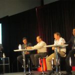
DAC: Tempus Lunchby Paul McLellan on 06-06-2013 at 4:03 pmCategories: Cadence, EDA
I had time for lunch on Monday. That is to say, there was a Cadence panel session about Has Timing Signoff Innovation has become and Oxymoron? What Happened and How Do We Fix It?
The moderator was Brian Fuller, lately of EE Times but now Editor-in-Chief at Cadence (I’m not sure quite what it means either). On the panel were Dipesh… Read More
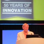
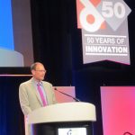
One new feature at DAC this year is that several of the keynotes are preceded by a ten minute vision of the future from one of the EDA CEOs. Today it was Wally Rhines’s turn. Wally is CEO of Mentor Graphics. He titled his talk Changing the World Through EDA. Since EDA as we know it started in the late 1970s, the number of transistors… Read More
As is now traditional, Gary Smith kicked off DAC proper (there were workshops earlier and some co-located conferences started days before). He started by dismissing the idea that it costs $170M to do an SoC design.
In fact he looked at 3 different cases. Firstly, the completely unconstrained design. Well, no design is completely… Read More
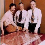
This year’s Kaufman award winner is Chenming Hu. In contrast to previous years, this was presented on the Sunday evening of DAC instead of at a separate event in San Jose. Chenming’s career was reviewed by Klaus Schuegraf, Group Vice President of EUV Product Development at Cymer, Inc (now part of ASML) and also one of… Read More
It has been a little over a fortnight since Paul Otellini officially stepped down from the CEO post and yet it seems to be more than a long time gone. Unlike his predecessors, he was not asked to remain on the board and perhaps it is a sign that his complete disengagement from the company was necessary to complete a future strategic engagement.… Read More
Fractal Technologies is a privately held EDA company with offices in San Carlos, California and Eindhoven, the Netherlands. The company was founded by a small group of highly recognized EDA professionals. The scope of Fractal Technologies is to check consistency and validate all different data formats used in your design and… Read More
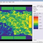
Thermal analysis has traditionally been given short shrift when compared to other more prominent issues facing chip designers. Invarian, to my eye at least, feels that the winds of change are in the air. Not that power or EM/IR issues will fade, that indeed is not the case and in fact quite the contrary, they are contributors to the… Read More


Enhancing Multi-Domain System Simulation with FMI Co-Simulation