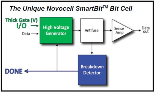
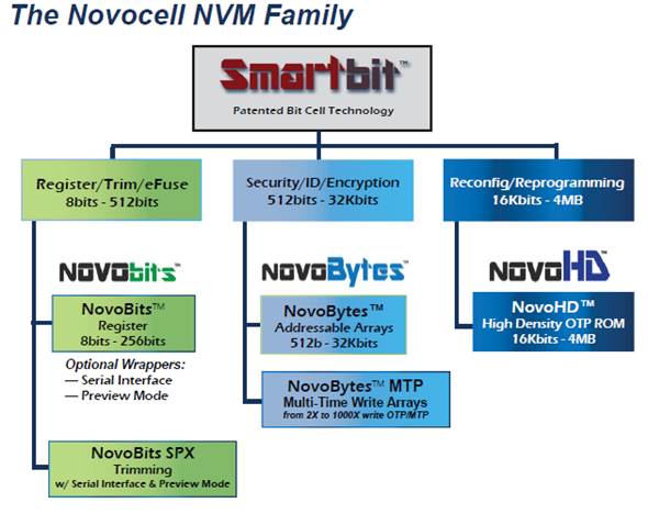
NVM IP offering from NovocellSemiconductor is based on SmartBit, an antifuse, One Time Programmable (OTP) technology, and the OTP block are embedded in standard Logic CMOS without any additional process or post process steps and can be programmed at the wafer level, in package, or in the field, as end user requires. What makes SmartBit technology unique is the “breakdown detector”, allowing to precisely determining when the voltage applied to the gate (allowing programming thememory cell by breaking the oxide and consequently allowing the current to flowthrough this oxide) will effectively have created an irreversible oxide breakdown, the “hard breakdown”, by opposition of a “soft breakdown” which is an apparent, reversible oxide breakdown. This is a first advantage: when the OTP programming step is completed, the user can be sure that every bit will have been set at the forecasted value. Apparently, this is not the case with each of the various OTP architectures, even if this is what you would naively expect from any NVM technology!

How do Novocell competitors proceed to program an OTP block, without this “breakdown detector” feature? They have to determine the“optimal programming timing” (the set time) provided to program each bit, which is determined for each specific foundry process (by technology node, and variation) and program the block according with this “set time”. Unfortunately, this ‘set time’ programming method will always result in some bits being ‘remnant’ bits un-programmed in the initial programming cycle. To be sure that every bit in the NVM block will have been set to the correct value, an additional programming cycle –at least- will be necessary to increase the yield. This approach is obviously time consuming (it takes at least twice the initial programming time), which can be pretty costly if, for example, you have to program the OTP using the tester, at wafer or packaged IC test step, when you consider the cost related to the test time on multi-million dollar devices. Another good point for SmartBit architecture: not only the programmingis more reliable, deterministic, but the cost of ownership linked to theprogramming step is cheaper.
Novocell competitors are trying to offer a safer approach, based on Error Correction circuitry or redundancy. Just take a look at what this precisely means, if we consider that some IP includes a full 2X redundancy of bits in order to achieve yield and performance requirements. Full redundancy can lead toeffectively doubling the area required on the chip for the customer-ordered bit density! A safer approach, even if it is theoretically not as safe as SmartBit, at the price of Silicon over cost. This over cost can be highly penalizing, when the NVM block is large and the device in production generating volumes that we see in the Consumer Electronic or Wireless Handset segments: million if not dozen of million units! Again, a costly tradeoff for an inferior programming methodology versus the Novocell dynamic approach based on “breakdown detection”…

Clearly, one of the Novocell’s differentiator is reliability, thanks to the “breakdown detector”. We also have seen that choosing SmartBit technology can dramatically reduce the total cost of ownership, by reducing programming time by a factor of 2 or more, and by using to a smaller NVM IP block size, leading to a smaller real estate or chip size than competitors, being forced to add redundancy to reach the same level of reliability – or yield.
Eric Estevefrom IPNEST –


Solving the EDA tool fragmentation crisis