You are currently viewing SemiWiki as a guest which gives you limited access to the site. To view blog comments and experience other SemiWiki features you must be a registered member. Registration is fast, simple, and absolutely free so please,
join our community today!
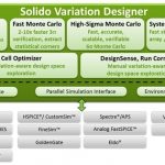
With the insatiable wafer appetites of the fabless semiconductor companies in the mobile space, yield has never been more critical. The result being better EDA tools every year and this blog highlights one of the many examples. It has been a pleasure writing about Solido Design Automation and seeing them succeed amongst the foundries… Read More
Many people are underestimating the speed and the magnitude of the transition that is about to take place with the tandem rollout of iOS 7 and the 64 bit A7 processor. While the former provides a nice visual upgrade to the entire ecosystem the latter will be used to collect accolades and drive application development that will result… Read More
If we check the many articles daily published in Semiwiki, I am sure that Moore’s Law has been mentioned every single day. There is a good reason why we constantly write about new technologies and advanced features like FinFet, FD-SOI, 450 mm wafers or double patterning: all of these are new challenges that the SC industry will have… Read More
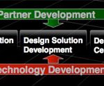
Recently, one of those very restrained press releases – in this case, Mentor Graphics and Imagination Technologiesextending their partnership for MIPS software support– crossed my desk with about 10% of the story. The 90% of this story I want to focus on is why Mentor is putting energy into this partnership… Read More
The amount of time spent debugging an SoC dwarfs the actual design time, with many engineering teams saying that debug and verification takes about 7X the effort as the actual design work. So any automation to reduce the amount of time spent in debug and verification would directly impact the product schedule in a big way.
An example… Read More
Founders
Cyril Spasevski is the President, CTO and founding engineer at Magillem, bringing a team of engineers, all experts with an SoC platform builder tool. In 2006 Cyril and his team met a seasoned business woman, and decided to form Magillem. Design teams were struggling with different tools at different stages of the flow,… Read More
The existence of TSMC’s Open Innovation Platform (OIP) program further sped up disaggregation of the semiconductor supply chain. Partly, this was enabled by the existence of a healthy EDA industry and an increasingly healthy IP industry. As chip designs had grown more complex and entered the system-on-chip (SoC) era, the amount… Read More
In the first post of this series, we named the popular methods for texture compression in OpenGL ES, particularly Imagination Technologies PVRTC on all Apple and many Android mobile devices. Now, let’s explore what texture compression involves, what PVRTC does, and how it differs from other approaches.… Read More
There was some serious backlash to the “Intel Bay Trail Fail” blog I posted last week, mostly personal attacks by the spoon fed Intel faithful, but there are however some very interesting points made amongst the 30+ comments so be sure and read them when you have a chance.
The Business insider article “The iPhone… Read More
Increasingly, a GPU is misnamed as a “graphics” processing unit. They are really specialized architecture highly parallel compute engines. You can use these compute engines for graphics, of course, but people are inventive and find ways of using GPUs for other tasks that can take advantage of the highly parallel… Read More


Enhancing Multi-Domain System Simulation with FMI Co-Simulation