You are currently viewing SemiWiki as a guest which gives you limited access to the site. To view blog comments and experience other SemiWiki features you must be a registered member. Registration is fast, simple, and absolutely free so please,
join our community today!
eMMC Mobile Memoryby Paul McLellan on 11-27-2013 at 11:40 amCategories: Arasan, IP
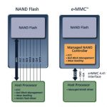
eMMC is the standard for mobile memory used in smartphones and tablets. The latest standard, released just this year, is eMMC 5.0. The previous standard, 4.51, was only released last year so things are moving quickly.
Arasan have a webinar next week to bring you up to speed on eMMC 5.0 in general and, of course, their own IP offering… Read More
To follow up my Bay Trail Fail blog which predicted that the leading edge Intel 22nm mobile SoC offering would fail, I must admit I was wrong. I did not think Bay Trail would see any traction in the tablet market but, as it turns out, Intel will ship 40M of those parts in 2014. Did you notice I said ship and not sell? Read on……… … Read More
Social Media at ARMby Daniel Payne on 11-26-2013 at 3:27 pmCategories: Arm, IP
The number one semiconductor IP company in the world is ARM, and they have really figured out how to use social media in a big way to communicate with and listen to their customers. When you first visit the Home page for ARM there are four social media icons displayed in monochrome underneath the menu bar. As you hover over the icons (Twitter,… Read More
The reader will find many updates in the “Interface IP Survey” from IPNEST, released in October 2013. Good question, as the IP market is a very fast moving one and the protocol based Interface IP, is moving even faster… exhibiting 20% growth rate in 2012, expected to grow with 10% CAGR between 2012 and 2017 to reach $700M. … Read More
There is always a lot of posturing and pontificating when semiconductor executives talk about the future of process development. They are fighting an air war of perception and investor expectations, so naturally want to make sure they have plenty to brag about. But, as we pointed out recently with Intel’s problems at 14nm, moving… Read More
Save closure time and boost performance by incorporating knowledge of physically aware design early into your front-end design implementation flow
With the adoption of advanced process nodes, design closure is becoming increasingly difficult due to the lack of convergence between the front end and the back end of the register-transfer… Read More
The Intel analyst meeting last week reads like an absolute train wreck with INTC stock dropping 5%+ the very next day. Since I work in the fabless semiconductor ecosystem during the day I was not able to listen to it live like the other pundits. Nor am I as easily fooled by Power Point slides. I did however review the materials and would… Read More
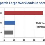
When you see a new product announcement from an EDA company, it is always put in terms that make it seem as if the engineer is sitting at his or her desktop with a big server and is running the new tool to wondrous effect. But the reality in the real world is that most companies have a computing infrastructure of server farms, often several… Read More
Yesterday Cadence had an all-day Signoff Summit where they talked about the tools that they have for signoff in advanced nodes. Well, of course, those tools work just fine in non-advanced nodes too, but at 20nm and 16nm there are FinFETs, double patterning, timing impacts from dummy metal fill, a gazillion corners to be analyzed… Read More
The first time that I saw a DRAM in a ceramic package running on a tester I made the mistake of touching my finger to the metal lid, scorching my finger and teaching me a lesson that ICs can run extremely hot. I’ve read a lot the past few years about 3D IC design, and immediately my mind becomes curious about how an engineer would go… Read More


Intel’s Pearl Harbor Moment